STM32F405xx, STM32F407xx
Electrical characteristics
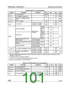
Table 35. Main PLL characteristics
Conditions
Symbol
fPLL_IN
Parameter
PLL input clock(1)
Min
Typ
Max
Unit
0.95(2)
24
1
-
2.10
168
MHz
MHz
fPLL_OUT
PLL multiplier output clock
48 MHz PLL multiplier output
clock
fPLL48_OUT
fVCO_OUT
-
48
75
MHz
MHz
PLL VCO output
192
75
100
-
-
-
432
200
300
-
VCO freq = 192 MHz
VCO freq = 432 MHz
tLOCK
PLL lock time
µs
-
RMS
25
peak
to
peak
Cycle-to-cycle jitter
Period Jitter
-
-
-
150
15
-
-
-
System clock
120 MHz
RMS
peak
to
200
Jitter(3)
ps
peak
Main clock output (MCO) for
RMII Ethernet
Cycle to cycle at 50 MHz
on 1000 samples
-
-
-
32
40
330
-
-
-
-
Main clock output (MCO) for MII Cycle to cycle at 25 MHz
Ethernet
on 1000 samples
Cycle to cycle at 1 MHz
on 1000 samples
Bit Time CAN jitter
VCO freq = 192 MHz
VCO freq = 432 MHz
0.15
0.45
0.40
0.75
(4)
IDD(PLL)
PLL power consumption on VDD
mA
mA
VCO freq = 192 MHz
VCO freq = 432 MHz
0.30
0.55
0.40
0.85
PLL power consumption on
VDDA
(4)
IDDA(PLL)
-
1. Take care of using the appropriate division factor M to obtain the specified PLL input clock values. The M factor is shared
between PLL and PLLI2S.
2. Guaranteed by design, not tested in production.
3. The use of 2 PLLs in parallel could degraded the Jitter up to +30%.
4. Based on characterization, not tested in production.
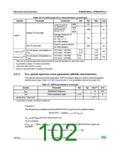
Table 36. PLLI2S (audio PLL) characteristics
Symbol
Parameter
Conditions
Min
Typ
Max
Unit
fPLLI2S_IN
fPLLI2S_OUT
fVCO_OUT
PLLI2S input clock(1)
0.95(2)
-
1
-
2.10
216
432
200
300
MHz
MHz
MHz
PLLI2S multiplier output clock
PLLI2S VCO output
192
75
-
VCO freq = 192 MHz
VCO freq = 432 MHz
-
tLOCK
PLLI2S lock time
µs
100
-
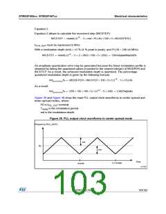
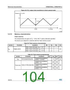
DocID022152 Rev 4
101/185

 STMICROELECTRONICS [ ST ]