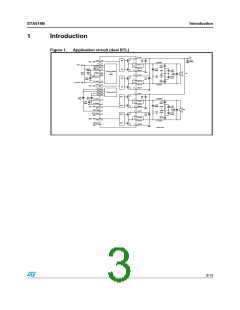
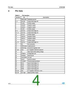
STA516B
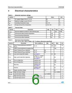
Electrical characteristics
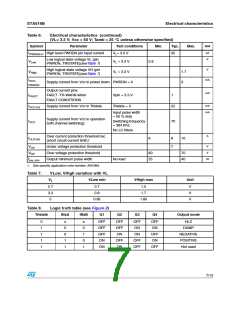
Table 6.
Symbol
Electrical characteristics (continued)
(VL= 3.3 V; Vcc = 50 V; Tamb = 25 °C unless otherwise specified)
Unit
µA
V
Parameter
Test conditions
Min.
Typ.
Max.
IPWRDN-H High level PWRDN pin input current
VL= 3.3 V
35
Low logical state voltage VL (pin
VLow
VL = 3.3 V
VL = 3.3 V
0.8
PWRDN, TRISTATE)(seeTable 7)
V
High logical state voltage VH (pin
VHigh
1.7
3
PWRDN, TRISTATE)(seeTable 7)
mA
IVCC-
Supply current from Vcc in power down PWRDN = 0
PWRDN
Output current pins
mA
IFAULT
FAULT -TH-WARN when
FAULT CONDITIONS
Vpin = 3.3 V
Tristate = 0
1
mA
mA
IVCC-hiz
Supply current from Vcc in Tristate
22
Input pulse width
= 50 % duty
Supply current from Vcc in operation
both channel switching)
IVCC
Switching frequency
= 384 Khz;
70
No LC filters
A
Over current protection threshold Isc
IOUT-SH
6
8
7
10
(short circuit current limit)1(1)
V
V
VUV
Under voltage protection threshold
Over voltage protection threshold
Output minimum pulse width
VOV
60
25
70
40
ns
tpw_min
No load
1. See specific application note number: AN1994.
Table 7.
VLow, VHigh variation with VL
VL
VLow min
VHigh max
Unit
2.7
3.3
5
0.7
0.8
1.5
1.7
V
V
V
0.85
1.85
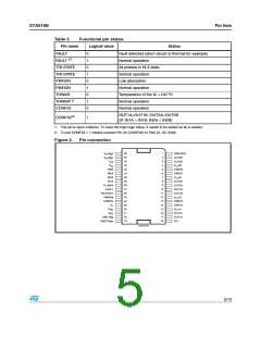
Table 8.
Logic truth table (see Figure 2)
Tristate
INxA
INxB
Q1
Q2
Q3
Q4
OFF
Output mode
0
1
1
1
1
x
0
0
1
1
x
0
1
0
1
OFF
OFF
OFF
ON
OFF
OFF
ON
OFF
ON
Hi-Z
ON
OFF
ON
DUMP
ON
NEGATIVE
POSITIVE
Not used
OFF
ON
OFF
OFF
ON
OFF
7/13

 STMICROELECTRONICS [ ST ]