STA516B
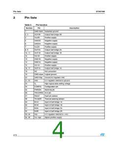
Pin lists
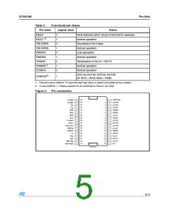
Table 3.
Pin name
Functional pin status
Logical value
Status
FAULT
0
1
0
1
0
1
0
1
0
Fault detected (short circuit or thermal for example)
Normal operation
FAULT (1)
TRI-STATE
TRI-STATE
PWRDN
PWRDN
THWAR
All powers in Hi-Z state
Normal operation
Low absorption
Normal operation
Temperature of the IC =130 oC
THWAR(1)
Normal operation
CONFIG
Normal operation
OUT1A=OUT1B; OUT2A=OUT2B
(IF IN1A = IN1B; IN2A = IN2B)
CONFIG(2)
1
1. The pin is open collector. To have the high logic value, it needs to be pulled up by a resistor.
2. To put CONFIG = 1 means connect Pin 24 (CONFIG) to Pins 21, 22 (Vdd)
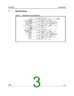
Figure 2.
Pin connection
36
35
34
33
32
31
30
29
28
27
26
25
24
23
22
21
20
19
1
2
V
CCSign
GND-SUB
OUT2B
OUT2B
VCC2B
VCCSign
VSS
3
4
VSS
5
IN2B
GND2B
GND2A
6
IN2A
7
IN1B
VCC2A
8
IN1A
OUT2A
OUT2A
OUT1B
OUT1B
9
TH_WAR
FAULT
TRI-STATE
PWRDN
CONFIG
10
11
12
13
14
15
16
17
18
V
CC1B
GND1B
GND1A
V
L
V
V
VCC1A
DD
DD
OUT1A
OUT1A
N.C.
GND-Reg
GND-Clean
D01AU1273
5/13

 STMICROELECTRONICS [ ST ]