Electrical characteristics
STA516B
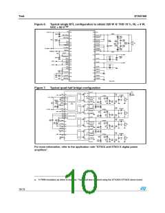
3
Electrical characteristics
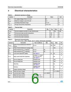
Table 4.
Symbol
Absolute maximum ratings
Parameter
Value
Unit
VCC
DC supply voltage (Pins 4,7,12,15)
Maximum voltage on pins 23 to 32
Operating temperature range
60
V
Vmax
Top
5.5
V
0 to 70
°C
°C
Tstg, Tj
Storage and junction temperature
-40 to 150
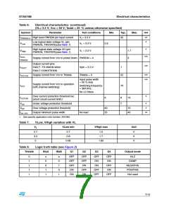
Table 5.
Symbol
Thermal data
Parameter
Min.
Typ.
Max.
2.5
Unit
Tj-case
TjSD
Twarn
thSD
Thermal resistance junction to case (thermal pad)
Thermal shut-down junction temperature
Thermal warning temperature
1
°C/W
°C
150
130
25
°C
Thermal shut-down hysteresis
°C
Table 6.
Electrical characteristics
(VL= 3.3 V; Vcc = 50 V; Tamb = 25 °C unless otherwise specified)
Unit
Symbol
Parameter
Test conditions
Min.
Typ.
Max.
mΩ
Power Pchannel/Nchannel MOSFET
RdsON
RdsON
Id=1A
200 240
100
µA
%
Idss
gN
Power Pchannel/Nchannel leakage Idss
Power Pchannel RdsON matching
Power Nchannel RdsON matching
Low current dead time (static)
Id=1A
95
95
%
gP
Id=1A
ns
ns
Dt_s
see Figure 4
10
20
50
L=22µH, C = 470nF
Rl = 8 Ω, Id=4.5A
see Figure 5
Dt_d
High current dead time (dynamic)
ns
ns
ns
td ON
Turn-on delay time
Turn-off delay time
Resistive load
Resistive load
100
100
td OFF
Resistive load
see Figure 4
tr
tf
Rise time
Fall time
25
ns
Resistive load
see Figure 4
25
52
V
V
VCC
Supply operating voltage
High level input voltage
Low level input voltage
High level Input current
Low level input current
10
VIN-High
VIN-Low
IIN-H
VL/2 +300mV
V
VL/2 -300mV
µA
µA
Pin voltage = VL
1
1
IIN-L
Pin voltage = 0.3 V
6/13

 STMICROELECTRONICS [ ST ]