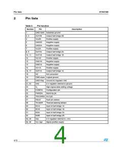
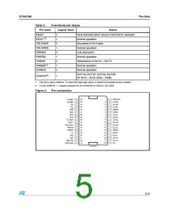
Pin lists
STA516B
2
Pin lists
Table 2.
Number
Pin function
Pin
Description
1
GND-SUB Substrate ground
2, 3
4
OUT2B
Vcc2B
GND2B
GND2A
Vcc2A
OUT2A
OUT1B
Vcc1B
GND1B
GND1A
Vcc1A
OUT1A
NC
Output half bridge 2B
Positive supply
5
Negative supply
Negative supply
Positive supply
6
7
8, 9
10, 11
12
Output half bridge 2A
Output half bridge 1B
Positive supply
13
Negative supply
Negative supply
Positive supply
14
15
16, 17
18
Output half bridge 1A
Not connected
19
GND-clean Logical ground
20
GND-Reg Ground for regulator Vdd
21, 22
23
Vdd
5 V regulator referred to ground
VL
High logical state setting voltage
Configuration pin
24
CONFIG
PWRDN
25
Stand-by pin
26
TRI-STATE Hi-Z pin
27
FAULT
TH-WAR
IN1A
Fault pin advisor
28
Thermal warning advisor
Input of half bridge 1A
Input of half bridge 1B
Input of half bridge 2A
Input of half bridge 2B
5 V regulator referred to +Vcc
Signal positive supply
29
30
IN1B
31
IN2A
32
IN2B
33, 34
35, 36
Vss
Vcc sign
4/13

 STMICROELECTRONICS [ ST ]