STA326
6 STA326 I2C BUS SPECIFICATION
The STA326 supports the I2C protocol. This protocol defines any device that sends data on to the bus as
a transmitter and any device that reads the data as a receiver. The device that controls the data transfer
is known as the master and the other as the slave. The master always starts the transfer and provides
the serial clock for synchronization. The STA326 is always a slave device in all of its communications.
6.1 COMMUNICATION PROTOCOL
6.1.1 Data Transition or change
Data changes on the SDA line must only occur when the SCL clock is low. SDA transition while the clock
is high is used to identify a START or STOP condition.
6.1.2 Start Condition
START is identified by a high to low transition of the data bus SDA signal while the clock signal SCL is
stable in the high state. A START condition must precede any command for data transfer.
6.1.3 Stop Condition
STOP is identified by a low to high transition of the data bus SDA signal while the clock signal SCL is stable
in the high state. A STOP condition terminates communication between STA326 and the bus master.
6.1.4 Data Input
During the data input the STA326 samples the SDA signal on the rising edge of clock SCL. For correct
device operation the SDA signal must be stable during the rising edge of the clock and the data can
change only when the SCL line is low.
6.2 DEVICE ADDRESSING
To start communication between the master and the STA326, the master must initiate with a start condi-
tion. Following this, the master sends 8-bits (MSB first) onto the SDA line corresponding to the device
select address and read or write mode.
The 7 most significant bits are the device address identifiers, corresponding to the I2C bus definition. In
the STA326 the I2C interface uses a device addresse of 0x34 or 0011010x.
The 8th bit (LSB) identifies read or write operation, RW. This bit is set to 1 in read mode and 0 for write
mode. After a START condition the STA326 identifies the device address on the bus. If a match is found,
it acknowledges the identification on the SDA bus during the 9th bit time. The byte following the device
identification byte is the internal space address.
6.3 WRITE OPERATION
Following the START condition the master sends a device select code with the RW bit set to 0. The
STA326 acknowledges this and then the master writes the internal address byte.
After receiving the internal byte address the STA326 again responds with an acknowledgement.
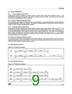
6.3.1 Byte Write
In the byte write mode the master sends one data byte. This is acknowledged by the STA326. The master
then terminates the transfer by generating a STOP condition.
6.3.2 Multi-byte Write
The multi-byte write modes can start from any internal address. Sequential data byte writes will be written
to sequential addresses within the STA326.
The master generating a STOP condition terminates the transfer.
8/43

 STMICROELECTRONICS [ ST ]