STA326
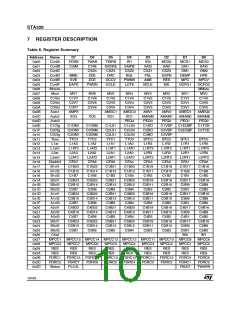
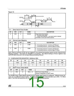
7.1 CONFIGURATION REGISTER A (Address 00h)
D7
FDRB
0
D6
TWAB
1
D5
TFRB
1
D4
IR1
0
D3
IR0
0
D2
MCS2
0
D1
MCS1
1
D0
MCS0
1
7.1.1 Master Clock Select
BIT
R/W
RST
NAME
DESCRIPTION
0
R/W
1
MCS0
Master Clock Select: Selects the ratio between the input
I2S sample frequency and the input clock.
1
2
R/W
R/W
1
0
MCS1
MCS2
The STA326 will support sample rates of 32kHz, 44.1kHz, 48Khz, 88.2kHz, and 96kHz. Therefore the
internal clock will be:
■ 32.768Mhz for 32kHz
■ 45.1584Mhz for 44.1khz, 88.2kHz, and 176.4kHz
■ 49.152Mhz for 48kHz, 96kHz, and 192kHz
The external clock frequency provided to the XTI pin must be a multiple of the input sample frequency (fs).
The correlation between the input clock and the input sample rate is determined by the status of the MCSx
bits and the IR (Input Rate) register bits. The MCSx bits determine the PLL factor generating the internal
clock and the IR bit determines the oversampling ratio used internally.
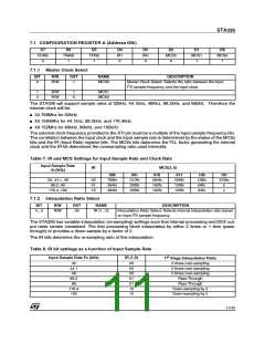
Table 7. IR and MCS Settings for Input Sample Rate and Clock Rate
Input Sample Rate
IR
MCS(2..0)
fs (kHz)
000
001
010
011
100
128fs
64fs
101
576fs
x
32, 44.1, 48
88.2, 96
00
01
1X
768fs
384fs
384fs
512fs
256fs
256fs
384fs
192fs
192fs
256fs
128fs
128fs
176.4, 192
64fs
x
7.1.2 Interpolation Ratio Select
BIT
R/W
RST
NAME
IR (1...0)
DESCRIPTION
4...3
R/W
00
Interpolation Ratio Select: Selects internal interpolation ratio based
on input I2S sample frequency
The STA326 has variable interpolation (re-sampling) settings such that internal processing and DDX out-
put rates remain consistent. The first processing block interpolates by either 2 times or 1 time (pass-
through) or provides a down-sample by a factor of 2.
The IR bits determine the re-sampling ratio of this interpolation.
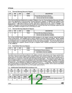
Table 8. IR bit settings as a function of Input Sample Rate
1st Stage Interpolation Ratio
2 times over-sampling
2 times over-sampling
2 times over-sampling
Pass-Through
Input Sample Rate Fs (kHz)
IR (1,0)
00
32
44.1
48
00
00
88.2
96
01
01
Pass-Through
176.4
192
10
Down-sampling by 2
Down-sampling by 2
10
11/43

 STMICROELECTRONICS [ ST ]