STA326
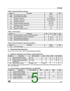
Table 3. Absolute Maximum Ratings
Symbol
VDD3
VDDA
Vi
Parameter
Value
-0.5 to 4
Unit
V
3.3V Digital Power Supply
3.3V Analog Power Supply
Voltage on input pins
-0.5 to 4
V
-0.5 to (VDD+0.5)
-0.5 to (VDD+0.5)
-40 to +150
-20 to +85
0 to +150
40
V
Vo
Voltage on output pins
V
Tstg
Storage Temperature
°C
°C
°C
V
Tamb
Tj
Ambient Operating Temperature
Operating Junction Temperature
DC Supply Voltage
VCC
VMAX
Maximum voltage on pins 20
5.5
V
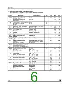
Table 4. Thermal Data
Symbol
Parameter
Min
Typ
Max
2.5
Unit
°C/W
°C
Rthj-case
Tj-SD
TWARN
Th-SD
Thermal resistance Junction to case (thermal pad)
Thermal Shut-down Junction Temperature
Thermal Warning Temperature
150
130
25
°C
Thermal Shut-down Hysteresis
°C
Table 5. Recommended Dc Operating Conditions
Symbol
Parameter
Value
Unit
VDD3
I/O Power Supply
3.0 to 3.6
V
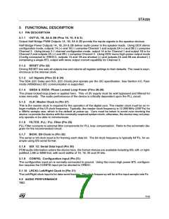
4 Electrical Characteristcs
(VDD3 = 3.3V 0.3V; Tamb = 25°C; unless otherwise specified)
4.1 GENERAL INTERFACE ELECTRICAL CHARACTERISTICS
Symbol
Parameter
Test Condition
Vi = 0V
Min.
Typ.
Max.
Unit
Note
Iil
Iih
Low Level Input no pull-up
High Level Input no pull-down
1
2
2
µA
µA
µA
1
1
1
Vi = VDD3
Vi = VDD3
IOZ
Tristate output leakage without
pullup/down
Vesd
Electrostatic Protection
Leakage < 1µA
2000
V
2
Note 1: The leakage currents are generally very small, < 1na. The values given here are maximum after an electrostatic stress on the pin.
Note 2: Human Body Model
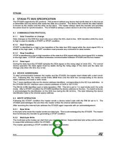
4.2 DC ELECTRICAL CHARACTERISTICS: 3.3V BUFFERS
Symbol
VIL
Parameter
Low Level Input Voltage
High Level Input Voltage
Schmitt Trigger Hysteresis
Low Level Output
Test Condition
Min.
Typ.
Max.
Unit
V
0.8
VIH
2.0
0.4
V
Vhyst
Vol
V
IoI = 2mA
0.15
V
Voh
High Level Output
Ioh = -2mA
VDD -0.15
V
5/43

 STMICROELECTRONICS [ ST ]