STA326
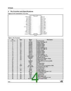
3 Pin Function and Specifications
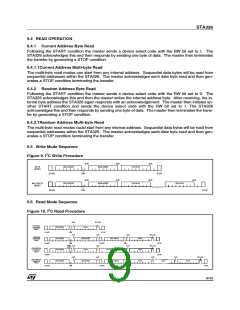
Figure 8. Pin Connection (Top view)
36
35
34
33
32
31
30
29
28
27
26
25
24
23
22
21
20
19
1
2
VCCSign
VSS
N.C.
N.C.
3
V
OUT2B
VCC2B
N.C.
DD
4
GND
BICKI
LRCKI
SDI
5
6
GND2B
GND2A
VCC2A
OUT2A
OUT1B
VCC1B
GND1B
GND1A.
N.C.
7
8
V
DDA
9
GNDA
XTI
10
11
12
13
14
15
16
17
18
PLL FILTER
RES
SDA
SCL
RESET
CONFIG
VL
VCC1A
OUT1A
GNDCLEAN
GND REG
V
DD REG
D04AU1540
Table 2. Pin Function
Pin
1, 2, 5, 14
3
Type
Name
N.C.
Description
Not Connected
Output half bridge 2B
Positive supply
Negative Supply
Negative Supply
Positive supply
Output half bridge 2A
Output half bridge 1B
Positive supply
O
I/O
I/O
I/O
I/O
O
OUT2B
VCC2B
GND2B
GND2A
VCC2A
OUT2A
OUT1B
VCC1B
GND1B
GND1A
VCC1A
OUT1A
GNDCLEAN
GNDREG
VREG1
VL
4
6
7
8
9
10
11
12
13
15
16
17
18
19
20
21
22
23
24
25
26
27
28
29
30
31
32
33
34
35
36
O
I/O
I/O
I/O.
I/O
O
I/O
I/O
I/O
I/O
I
Negative Supply
Negative Supply
Positive supply
Output half bridge 1A
Logic reference ground
Substrate ground
Internal +5V regulator voltage
Digital Supply 3.3V
Configuration pin (mono parallel)
Reset
CONFIG
RESET
SCL
I
I
I²C Serial Clock
I²C Serial Data
I/O
RES
I
SDA
Reserved
PLL FILTER
XTI
GNDA
VDDA
SDI_12
LRCKI
BICKI
GND
VDD
VSS
VCCSIGN
This pin must be connected to GND
Connection to PLL filter
PLL Input Clock
I
I/O
I/O
I
I/O
I
I/O
I/O
I/O
I/O
Analog Ground
Analog Supply 3.3
I²S Serial Data Channels 1 & 2
I²S Left/Right Clock,
I²S Serial Clock
Digital Ground
Digital Supply 3.3V
Internal - 5V (Relative to Vcc)
Internal signal supply
4/43

 STMICROELECTRONICS [ ST ]