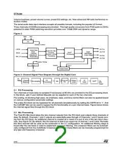
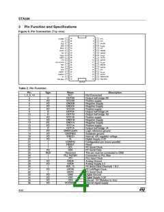
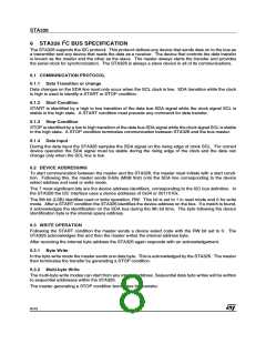
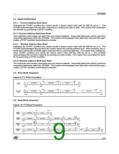
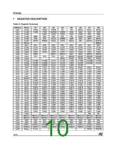
STA326
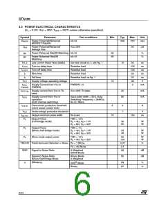
4.3 POWER ELECTRICAL CHARACTERISTCS
(VL = 3.3V; Vcc = 30V; Tamb = 25°C unless otherwise specified)
Symbol
Parameter
Test conditions
Min.
Typ.
Max.
Unit
RdsON Power Pchannel/Nchannel
MOSFET RdsON
Id=1A
200
270
mΩ
Idss
Power Pchannel/Nchannel
leakage Idss
Vcc=35V
50
µA
gN
gP
Power Pchannel RdsON Matching Id=1A
95
95
%
%
Power Nchannel RdsON
Matching
Id=1A
Dt_s
td ON
td OFF
tr
Low current Dead Time (static)
Turn-on delay time
Turn-off delay time
Rise time
see test circuit no.1; see fig. 1
Resistive load
10
20
100
100
25
ns
ns
ns
ns
ns
V
Resistive load
Resistive load
tf
Fall time
Resistive load; as fig. 1
25
VCC
Supply voltage operating voltage
10
36
IVCC-
PWRDN
Supply Current from Vcc in
PWRDN
PWRDN = 0
3
mA
IVCC-hiz Supply current from Vcc in Tri-
state
Vcc=30V; Tri-state
22
80
mA
mA
IVCC
Supply current from Vcc in
operation
Input pulse width = 50% Duty;
Switching Frequency = 384Khz;
No LC filters;
(both channel switching)
Iout-sh
VUV
Overcurrent protection threshold
(short circuit current limit)
4
6
7
A
Undervoltage protection threshold
V
tpw-min Output minimum pulse width
No Load
70
150
ns
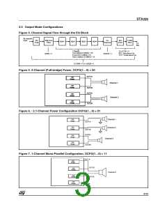
Po
Po
Po
Output Power
(Full-bridge mode)
THD = 10%
RL = 4Ω; VS = 17V
RL = 8Ω; VS = 32V
30
60
W
W
Output Power
(Binary half-bridge mode)
THD = 1%
RL = 4Ω; VS = 17V
RL = 8Ω; VS = 32V
25
46
W
W
Mono mode output power
THD = 10%
RL = 4Ω; VS = 32V
60
120
W
W
THD+N Total Harmonic Distortion + Noise Po = 1 Wrms
Po = 40 Wrms
0.07
0.1
99
%
SNR
Signal to Noise Ratio
A-Weighted
DDX® Mode
dB
dB
Signal to Noise Ratio,
Binary Half-Bridge Mode
Binary Mode
A-Weighted
92
DDX® Mode
Binary
η
Efficiency
89
87
%
%
6/43

 STMICROELECTRONICS [ ST ]