STA326
7.1.3 Thermal Warning Recovery Bypass
BIT
R/W
RST
NAME
DESCRIPTION
5
R/W
1
TWRB
Thermal-Warning Recovery Bypass:
0 – Thermal warning Recovery enabled
1 – Thermal warning Recovery disabled
If the Thermal Warning Adjustment is enabled (TWAB=0), then the Thermal Warning Recovery will deter-
mine if the adjustment is removed when Thermal Warning is negative. If TWRB=0 and TWAB=0, then
when a thermal warning disappears the gain adjustment determined by the Thermal Warning Post-
Scale(default = -3dB) will be removed and the gain will be added back to the system. If TWRB=1 and
TWAB=0, then when a thermal warning disappears the Thermal Warning Post-Scale gain adjustment will
remain until TWRB is changed to zero or the device is reset.
7.1.4 Thermal Warning Adjustment Bypass
BIT
R/W
RST
NAME
DESCRIPTION
6
R/W
1
TWAB
Thermal-Warning Adjustment Bypass:
0 – Thermal warning adjustment enabled
1 – Thermal warning adjustment disabled
The on-chip STA326 Power Output block provides feedback to the digital controller using inputs to the
Power Control block. The TWARN input is used to indicate a thermal warning condition. When TWARN
is asserted (set to 0) for a period greater than 400ms, the power control block will force an adjustment to
the modulation limit in an attempt to eliminate the thermal warning condition. Once the thermal warning
volume adjustment is applied, whether the gain is reapplied when TWARN is de-asserted is dependent
on the TWRB bit.
7.1.5 Fault Detect Recovery Bypass
BIT
R/W
RST
NAME
DESCRIPTION
Fault Detector Recovery Bypass:
7
R/W
0
FDRB
0 – Fault Detector Recovery enabled
1 – Fault Detector Recovery disabled
The DDX Power block provides feedback to the digital controller using inputs to the Power Control block.
The FAULT input is used to signal a fault condition (either over-current or thermal). When FAULT is as-
serted (set to 0), the power control block will attempt automatic recovery from the fault by asserting the tri-
state signal in a sequence to reset the fault and retest the fault status. The sequence period can range
from 0.1 milliseconds to 1 second as defined by the Fault-Detect Recovery Constant register (FDRC reg-
isters 29-2Ah). This sequence is repeated for as long as the fault condition exists. This feature is enabled
by default but can be disabled by setting the FDRB control bit to 1. If Fault-Detect Recovery is disabled
(not recommended), an output stage FAULT will cause a shut-down condition, which must be reset either
by toggling the external reset pin or via a VCC power cycle to the IC.
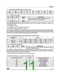
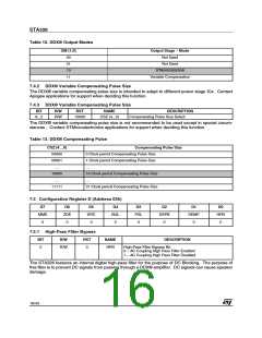
7.2 CONFIGURATION REGISTER B (Address 01h)
D7
C1IM
1
D6
C1IM
0
D5
DSCKE
0
D4
SAIFB
0
D3
SAI3
0
D2
SAI2
0
D1
SAI1
0
D0
SAI0
0
7.2.1 Serial Audio Input Interface Format
BIT
R/W
RST
NAME
DESCRIPTION
3…0
R/W
0000
SAI (3...0)
Serial Audio Input Interface Format: Determines the interface format of
the input serial digital audio interface.
12/43

 STMICROELECTRONICS [ ST ]