STA326
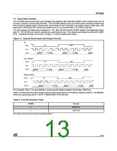
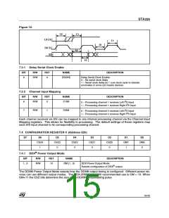
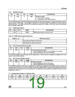
Figure 12.
T2
T3
LRCKI
T1
T0
BICKI
T4
SDI
T5
7.3.1 Delay Serial Clock Enable
BIT
R/W
RST
NAME
DESCRIPTION
5
R/W
0
DSCKE
Delay Serial Clock Enable:
0 – No serial clock delay
1 – Serial clock delay by 1 core clock cycle to tolerate
anomalies in some I2S master devices
7.3.2 Channel Input Mapping
BIT
R/W
RST
NAME
DESCRIPTION
0 – Processing channel 1 receives Left I2S Input
1 – Processing channel 1 receives Right I2S Input
6
R/W
0
C1IM
0 – Processing channel 2 receives Left I2S Input
1 – Processing channel 2 receives Right I2S Input
7
R/W
1
C2IM
Each channel received via I2S can be mapped to any internal processing channel via the Channel Input
Mapping registers. This allows for flexibility in processing. The default settings of these registers map
each I2S input channel to its corresponding processing channel.
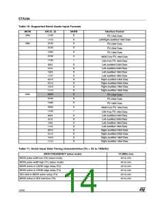
7.4 CONFIGURATION REGISTER C (Address 02h)
D7
D6
CSZ4
1
D5
CSZ3
0
D4
CSZ2
0
D3
CSZ1
0
D2
CSZ0
0
D1
OM1
1
D0
OM0
0
7.4.1 DDX® Power Output Mode
BIT
R/W
RST
NAME
OM (1...0)
DESCRIPTION
1...0
R/W
10
DDX Power Output Mode:
Selects configuration of DDX® output.
The DDX® Power Output Mode selects how the DDX® output timing is configured. Different power de-
vices can use different output modes. The DDX-2060/2100/2160 recommended use is OM = 10. When
OM=11 the CSZ bits determine the size of the DDX® compensating pulse.
15/43

 STMICROELECTRONICS [ ST ]