ST92F124/F150/F250 - INTERRUPTS
5.6 EXTERNAL INTERRUPTS
The ST9 core contains 8 external interrupt sources
grouped into four pairs.
Figure 51 and Table 20 give an overview of the ex-
ternal interrupts and vectors.
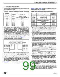
Table 19. External Interrupt Channel Grouping
External
Table 20. Multiplexed Interrupt Sources
External
Channel
Internal Interrupt Source
Channel
I/O Port Pin
Interrupt
Interrupt
INTA0
INTA1
INTB0
INTB1
INTC0
INTC1
INTD0
INTD1
Timer/Watchdog
Standard Timer
INT0
P8[1:0] P7[7:5]
P6[7,5] P5[7:5, 2:0] P4[7,4]
WKUP[0:15]
INTD1
INT1
INT6
INT5
INT4
INT3
INT2
INT1
INT0
INTD0
INTC1
INTC0
INTB1
INTB0
INTA1
INTA0
P6.1
P6.3
P6.2
P6.3
P6.2
P6.0
P6.0
Extended Function Timer 0
INT2
Extended Function Timer 1
INT3
3 TM
E
/Flash
INT4
SPI Interrupt
RCCU
INT5
INT6
Wake-up Management Unit
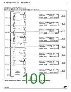
Each source has a trigger control bit TEA0,..TED1
(R242,EITR.0,..,7 Page 0) to select triggering on
the rising or falling edge of the external pin. If the
Trigger control bit is set to “1”, the corresponding
pending bit IPA0,..,IPD1 (R243,EIPR.0,..,7 Page
0) is set on the input pin rising edge, if it is cleared,
the pending bit is set on the falling edge of the in-
put pin. Each source can be individually masked
– The source of INTA0 can be selected between
the external pin INT0 or the Timer/Watchdog pe-
ripheral using the IA0S bit in the EIVR register
(R246 Page 0).
– The source of INTA1 can be selected between
the external pin INT1 or the Standard Timer us-
ing the INTS bit in the STC register (R232 Page
11).
through
the
corresponding
control
bit
IMA0,..,IMD1 (EIMR.7,..,0). See Figure 51.
– The source of INTB0 can be selected between
the external pin INT2 or the on-chip Extended
Function Timer 0 using the EFTIS bit in the CR3
register (R255 Page 28).
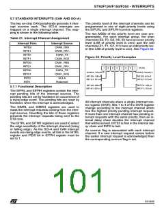
Figure 50. Priority Level Examples
PL2D PL1D PL2C PL1C PL2B PL1B PL2A PL1A
– The source of INTB1 can be selected between
external pin INT3 or the on-chip Extended Func-
tion Timer 1 using the EFTIS bit in the CR3 reg-
ister (R255 Page 29).
1
0
0
0
1
0
0
1
EIPLR
SOURCE PRIORITY
SOURCE PRIORITY
INT.D0: 100=4
INT.D1: 101=5
INT.A0: 010=2
INT.A1: 011=3
– The source of INTC0 can be selected between
external pin INT4 or the On-chip E3 TM/Flash
Memory using bit FEIEN in the ECR register (Ad-
dress 224001h).
INT.C0: 000=0
INT.C1: 001=1
INT.B0: 100=4
INT.B1: 101=5
– The source of INTC1 can be selected between
external pin INT5 or the on-chip SPI using the
SPIS bit in the SPCR0 register (R241 Page 7).
The priority level of the external interrupt sources
can be programmed among the eight priority lev-
els with the control register EIPLR (R245). The pri-
ority level of each pair is software defined using
the bits PRL2,PRL1. For each pair, the even chan-
nel (A0,B0,C0,D0) of the group has the even prior-
ity level and the odd channel (A1,B1,C1,D1) has
the odd (lower) priority level.
– The source of INTD0 can be selected between
external pin INT6 or the Reset and Clock Unit
RCCU using the INT_SEL bit in the CLKCTL reg-
ister (R240 Page 55).
– The source of INTD1 can be selected between
the NMI pin and the WUIMU Wakeup/Interrupt
Lines using the ID1S bit in the WUCRTL register
(R248 Page 9).
Figure 50 shows an example of priority levels.
Warning: When using external interrupt channels
shared by both external interrupts and peripherals,
special care must be taken to configure control
registers both for peripheral and interrupts.
99/426
9

 STMICROELECTRONICS [ ST ]