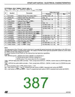
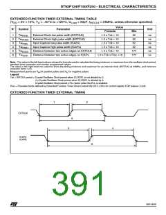
ST92F124/F150/F250 - ELECTRICAL CHARACTERISTICS
EXTERNAL BUS TIMING TABLE (MC=1)
(V = 5V ± 10%, T = –40°C to +125°C, C
= 0 to 50pF
DD
N°
A
Load
Value (see note)
Symbol
Parameter
Unit
Formula
Min
160
10
Max
1
2
3
4
5
6
7
8
9
TsA (ALE)
ThALE (A)
TwALE
Address Set-up Time before ALE ↓
Address Hold Time after ALE ↓
ALE High Pulse Width
Tck*Wa+TckH - 48
TckL - 31
ns
ns
ns
ns
ns
ns
ns
ns
ns
ns
ns
ns
ns
ns
ns
ns
ns
Tck*Wa+TckH - 58
0
150
0
TdAz (OEN)
TdOEN(Az)
TwOEN
Address Float (P0) to OEN ↓
P0 driven after OEN ↑
TckL - 13
29
OEN Low Pulse Width
Tck*Wd+TckH - 36
Tck*Wd+TckH - 36
Tck*Wd+TckH - 44
0
172
172
TwWEN
WEN Low Pulse Width
TdOEN (DR)
ThDR (OEN)
OEN ↓ to Data Valid Delay
Data hold time after OEN ↑
Address (A21:A8) hold time after OEN ↑
Address (A21:A8) hold time after WEN ↑
Address (A21:A0) valid to OEN ↑
Address (A21:A0) valid to WEN ↑
Data Set-up time before WEN ↑
Data Hold Time after WEN ↑
ALE ↑ to WEN ↑ Delay
164
0
0
10 ThOEN(A)
11 ThWEN(A)
12 TvA(OEN)
0
0
0
Tck (Wd+Wa+1.5) - 76
Tck (Wd+Wa+1.5) - 44
Tck*Wd+TckH - 158
TckL - 37
382
414
50
5
13 TvA(WEN)
14 TsD (WEN)
15 ThWEN(DW)
16 TdALE (WEN)
17 TdALE (OEN)
Tck (Wd+Wa+1.5) - 54
Tck (Wd+Wa+1.5) - 50
404
408
ALE ↑ to OEN ↑ Delay
Notes:
The expressions in the “Formula” column show how to calculate the typical parameter value depending on the CPU clock
period and the number of inserted wait cycles. The values in the Min column give the parameter values for a CPU clock
at 12MHz and two wait states for T1 and T2.
For certain versions of the ST92F150, the external bus has high-drive capabilities.
Legend:
Tck = INTCLK period = OSCIN period when OSCIN is not divided by 2;
= 2*OSCIN period when OSCIN is divided by 2;
= OSCIN period / PLL factor when the PLL is enabled
TckH = INTCLK high pulse width (normally = Tck/2, except when INTCLK = OSCIN, in which case it is OSCIN high pulse
width)
TckL = INTCLK low pulse width (normally = Tck/2, except when INTCLK = OSCIN, in which case it is OSCIN low pulse
width)
P = clock prescaling value (=PRS; division factor = 1+P)
Wa = wait cycles on ALE; = max (P, programmed wait cycles in EMR2, requested wait cycles with WAIT)
Wd = wait cycles on OEN and WEN ; = max (P, programmed wait cycles in WCR, requested wait cycles with WAIT)
387/426
1

 STMICROELECTRONICS [ ST ]