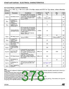
ST92F124/F150/F250 - ELECTRICAL CHARACTERISTICS
11 ELECTRICAL CHARACTERISTICS
This product contains devices to protect the inputs
against damage due to high static voltages, how-
ever it is advisable to take normal precautions to
avoid application of any voltage higher than the
specified maximum rated voltages.
Power Considerations. The average chip-junc-
tion temperature, T , in Celsius can be obtained
J
from:
T =
T + P x RthJA
A D
J
Where: T =
Ambient Temperature.
A
For proper operation it is recommended that V
IN
RthJA = Package thermal resistance
(junction-to ambient).
and V be higher than V and lower than V .
DD
O
SS
Reliability is enhanced if unused inputs are con-
nected to an appropriate logic voltage level (V
P =
P
+ P
.
PORT
DD
D
INT
or V ).
SS
P
P
=
I
x V (chip internal power).
INT
PORT
DD DD
=Port power dissipation
(determined by the user)
ABSOLUTE MAXIMUM RATINGS
Symbol
Parameter
Value
Unit
V
V
Supply Voltage
– 0.3 to 6.5
DD
AV
AV
ADC Reference Voltage
ADC Ground
V
to V + 0.3
V
DD
SS
IN
SS
DD
V
SS
V
Input Voltage (all pins except pure open drain I/O pins)
Input Voltage (pure open drain I/O pins)
Analog Input Voltage (ADC inputs)
Storage Temperature
– 0.3 to V + 0.3
V
V
DD
V
– 0.3 to 6.5
INOD
V
-0.3 to AV + 0.3
V
AIN
DD
T
– 55 to +150
°C
mA
mA
mA
STG
(2)
⎥I
⎥
Load Current
10
IO
(1)
(2)
⎥I
⎥
Pin Injection Current - Digital and Analog Inputs
10
INJ
(2)
⎥I
⎥
Absolute sum of all Pin Injection Current in the device
100
TINJ
Notes:
Stresses above those listed as “absolute maximum ratings“ may cause permanent damage to the device. This is a stress rating only and
functional operation of the device at these conditions is not implied. Exposure to maximum rating conditions for extended periods may affect
device reliability. All voltages are referenced to V = 0 V.
SS
Note 1: Pin injection current occurs when the voltage on any pin exceeds the specified range.
Note 2: Value guaranteed by design.
THERMAL CHARACTERISTICS
Symbol
Package
Value
Unit
TQFP64
PQFP100
TQFP100
47
28
44
RthJA
°C/W
374/426
1

 STMICROELECTRONICS [ ST ]