J1850 Byte Level Protocol Decoder (JBLPD)
J1850 BYTE LEVEL PROTOCOL DECODER (Cont’d)
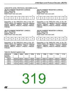
These registers are structured in eight groups of
four registers. The user can gain access to these
registers programming the RSEL[2:0] bits of the
OPTIONS register while the RSEL[3] bit of the
same register must be placed at 1. In this way the
user can select the group where the registers that
he/she wants to use are placed. See the descrip-
tion of OPTIONS register for the correspondence
between registers and the values of RSEL[2:0] bits
(See Table 62).
register and the RDRF flag is set. Also, every other
data byte received in this frame is transferred to
the RXDATA register unless the JBLPD peripheral
is put into sleep mode setting the SLP bit.
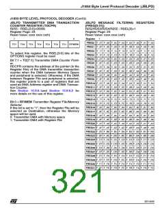
If the bit of the array correspondent to the I.D. byte
is clear, then the transfer of this byte as well as any
byte for the balance of this frame is inhibited, and
the RDRF bit remains cleared.
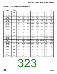
The bit 0 of the FREG[0] register (FREG[0].0 -
marked as F_00 in the previous table) corre-
sponds to the I.D. byte equal to 00h while the bit 7
of the FREG[31] register (FREG[31].7 - marked as
F_FF in the previous table) corresponds to the I.D.
byte equal to FFh.
From the functional point of view, the FREG[0]-
FREG[31] registers can be seen as an array of
256 bits involved in the J1850 received message
filtering system.
The first byte received in a frame (following a valid
received SOF character) is an Identifier (I.D.) byte.
It is used by the JBLPD peripheral as the address
of the 256 bits array.
Note: The FREG registers are undefined upon re-
set. Because of this, it is strongly recommended
that the contents of these registers has to be de-
fined before JE is set for the first time after reset.
Otherwise, unpredictable results may occur.
If the bit of the array correspondent to the I.D. byte
is set, then the byte is transferred to the RXDATA
322/426
9

 STMICROELECTRONICS [ ST ]