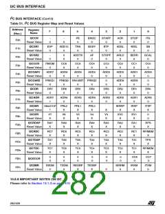
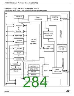
J1850 Byte Level Protocol Decoder (JBLPD)
J1850 BYTE LEVEL PROTOCOL DECODER (Cont’d)
10.9.3.2 Transmitting Messages
chronize off the decoder output to time the VPWO
symbol time.
This section describes the general procedures
used by the JBLPD to successfully transmit J1850
frames of data out the VPWO pin. The first five
sub-sections describe the procedures used for
transmitting the specific transmit data types. The
last section goes into the details of the transmitted
symbol timing, synchronizing of symbols received
from the external J1850 bus, and how data bit ar-
bitration works.
A detailed description of the JBLPD opcodes can
be find in the description of the OP[2:0] bits in the
TXOP register.
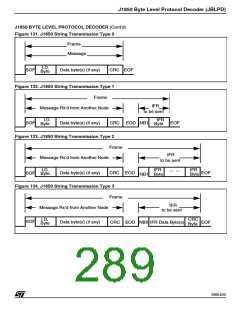
Message Byte String Transmission (Type 0
IFR)
Message byte transmitting is the outputting of data
bytes on the VPWO pin that occurs subsequent to
a received bus idle condition. All message byte
strings start with a SOF symbol transmission, then
one or more data bytes are transmitted. A CRC
byte is then transmitted followed by an EOD sym-
bol (see Figure 131) to complete the transmission.
If transmission is queued while another frame is
being received, then the JBLPD will time an Inter-
Frame Separation (IFS) time (Tv6) before com-
mencing with the SOF character.
The important concept to note for transmitting data
is: the activity sent over the VPWO line should be
timed with respect to the levels and transitions
seen on the filtered VPWI line.
The J1850 bus is a multiplexed bus, and the
VPWO & VPWI pins interface to this bus through a
transceiver I.C. Therefore, the propagation delay
through the transceiver I.C. and external bus filter-
ing must be taken into account when looking for
transmitted edges to appear back at the receiver.
The external propagation delay for an edge sent
out on the VPWO line, to be detected on the VPWI
The user program will decide at some point that it
wants to initiate a message byte string. The user
program writes the TXDATA register with the first
message data byte to be transmitted. Next, the
TXOP register is written with the MSG opcode if
more than one data byte is contained within the
message, or with MSG+CRC opcode if one data
byte is to be transmitted. The action of writing the
TXOP register causes the TRDY bit to be cleared
signifying that the TXDATA register is full and a
corresponding opcode has been queued. The
JBLPD must wait for an EOF nominal time period
at which time data is transferred from the TXDATA
register to the transmit shift register. The TRDY bit
is again set since the TXDATA register is empty.
line is denoted as T
tween 0 and 31 µs nominal via the JDLY[4:0] bits
in CONTROL register.
and is programmable be-
p-ext
The transmitter VPW encoder sets the proper level
to be sent out the VPWO line. It then waits for the
corresponding level transition to be reflected back
at the VPW decoder input.
Taking into account the external loop delay (T
)
p-ext
and the digital filter delay, the encoder will time its
output to remain at this level so that the received
symbol is at the correct nominal symbol time (refer
to “Transmit Opcode Queuing” section). If arbitra-
tion is lost at any time during bit 0 or bit 1 transmis-
sion, then the VPWO line goes passive. At the end
of the symbol time on VPWO, the encoder chang-
es the state of VPWO if any more information is to
be transmitted. It then times the new state change
from the receiver decoder output.
The JBLPD should also begin transmission if an-
other device begins transmitting early. As long as
an EOF minimum time period elapses, the JBLPD
should begin timing and asserting the SOF symbol
with the intention of arbitrating for the bus during
the transmission of the first data byte. If a transmit
is requested during an incoming SOF symbol, the
JBLPD should be able to synchronize itself to the
incoming SOF up to a time of Tv1 max. (96 µs) into
the SOF symbol before declaring that it was too
late to arbitrate for this frame.
Note that depending on the symbol (especially the
SOF, NB0, NB1 symbols) the decoder output may
actually change to the desired state before the
transmit is attempted. It is important to still syn-
286/426
9

 STMICROELECTRONICS [ ST ]