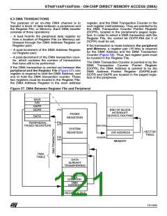
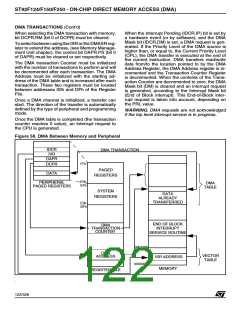
ST92F124/F150/F250 - RESET AND CLOCK CONTROL UNIT (RCCU)
7 RESET AND CLOCK CONTROL UNIT (RCCU)
7.1 INTRODUCTION
the PLL multiplier circuit. The resulting signal,
CLOCK2, is the reference input clock to the pro-
grammable Phase Locked Loop frequency multi-
plier, which is capable of multiplying the clock fre-
quency by a factor of 6, 8, 10 or 14; the multiplied
clock is then divided by a programmable divider,
by a factor of 1 to 7. By these means, the ST9 can
operate with cheaper, medium frequency (3-5
MHz) crystals, while still providing a high frequen-
cy internal clock for maximum system perform-
ance; the range of available multiplication and divi-
sion factors allow a great number of operating
clock frequencies to be derived from a single crys-
tal frequency.
The Reset and Clock Control Unit (RCCU) com-
prises two distinct sections:
– the Clock Control Unit, which generates and
manages the internal clock signals.
– the Reset/Stop Manager, which detects and
flags Hardware, Software and Watchdog gener-
ated resets.
On ST9 devices where the external Stop pin and/
or the Wake-Up Interrupt Manager Unit are availa-
ble, this circuit also detects and manages the Stop
mode during which all oscillators are frozen in or-
der to achieve the lowest possible power con-
sumption (refer to the Reset/Stop mode and
Wake-Up Interrupt Manager Unit description).
For low power operation, especially in Wait for In-
terrupt mode, the Clock Multiplier unit may be
turned off, whereupon the output clock signal may
be programmed as CLOCK2 divided by 16. For
further power reduction, a low frequency external
clock connected to the CK_AF pin may be select-
ed, whereupon the crystal controlled main oscilla-
tor may be turned off.
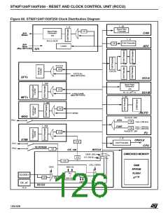
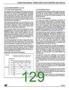
7.2 CLOCK CONTROL UNIT
The Clock Control Unit generates the internal
clocks for the CPU core (CPUCLK) and for the on-
chip peripherals (INTCLK). The Clock Control Unit
may be driven by the on-chip oscillator (provided
an external crystal circuit is connected to the OS-
CIN and OSCOUT pins), or by an external pulse
generator, connected to OSCOUT (see Figure 66
and Figure 68). When significant power reduction
is required, a low frequency external clock may be
selected. To do this, this clock source must be
connected to the CK_AF pin.
The internal system clock, INTCLK, is routed to all
on-chip peripherals, as well as to the programma-
ble Clock Prescaler Unit which generates the clock
for the CPU core (CPUCLK). (See Figure 59)
The Clock Prescaler is programmable and can
slow the CPU clock by a factor of up to 8, allowing
the programmer to reduce CPU processing speed,
and thus power consumption, while maintaining a
high speed clock to the peripherals. This is partic-
ularly useful when little actual processing is being
done by the CPU and the peripherals are doing
most of the work.
7.2.1 Clock Control Unit Overview
As shown in Figure 59 a programmable divider
can divide the CLOCK1 input clock signal by two.
In practice, the divide-by-two is virtually always
used in order to ensure a 50% duty cycle signal to
Figure 59. Clock Control Unit Simplified Block Diagram
1/16
CPUCLK
to
CPU Core
CPU Clock
Prescaler
PLL
Clock Multiplier
Crystal
oscillator
/Divider Unit
1/2
CLOCK2
CLOCK1
CK_AF
INTCLK
to
CK_AF
source
Peripherals
125/426
9

 STMICROELECTRONICS [ ST ]