ST92F124/F150/F250 - ON-CHIP DIRECT MEMORY ACCESS (DMA)
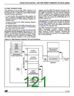
6.3 DMA TRANSACTIONS
The purpose of an on-chip DMA channel is to
transfer a block of data between a peripheral and
the Register File, or Memory. Each DMA transfer
consists of three operations:
register, and the DMA Transaction Counter in the
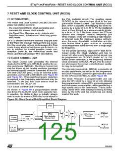
next register (odd address). They are pointed to by
the DMA Transaction Counter Pointer Register
(DCPR), located in the peripheral’s paged regis-
ters. In order to select a DMA transaction with the
Register File, the control bit DCPR.RM (bit 0 of
DCPR) must be set.
– A load from/to the peripheral data register to/
from a location of Register File (or Memory) ad-
dressed through the DMA Address Register (or
Register pair)
If the transaction is made between the peripheral
and Memory, a register pair (16 bits) is required
for the DMA Address and the DMA Transaction
Counter (Figure 58). Thus, two register pairs must
be located in the Register File.
– A post-increment of the DMA Address Register
(or Register pair)
– A post-decrement of the DMA transaction coun-
ter, which contains the number of transactions
that have still to be performed.
The DMA Transaction Counter is pointed to by the
DMA Transaction Counter Pointer Register
(DCPR), the DMA Address is pointed to by the
DMA Address Pointer Register (DAPR),both
DCPR and DAPR are located in the paged regis-
ters of the peripheral.
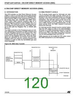
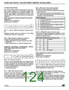
If the DMA transaction is carried out between the
peripheral and the Register File (Figure 57), one
register is required to hold the DMA Address, and
one to hold the DMA transaction counter. These
two registers must be located in the Register File:
the DMA Address Register in the even address
Figure 57. DMA Between Register File and Peripheral
IDCR
IVR
DAPR
FFh
END OF BLOCK
INTERRUPT
SERVICE ROUTINE
DCPR
PAGED
DATA
REGISTERS
F0h
EFh
PERIPHERAL
PAGED REGISTERS
000100h
000000h
SYSTEM
VECTOR
TABLE
ISR ADDRESS
MEMORY
REGISTERS
E0h
DFh
DMA
TABLE
DATA
ALREADY
TRANSFERRED
DMA
COUNTER
DMA
ADDRESS
REGISTER FILE
121/426
9

 STMICROELECTRONICS [ ST ]