Electrical characteristics
ST10F276E
Unit
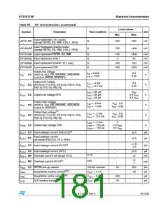
Table 90. DC characteristics (continued)
Limit values
Min.
Symbol
Parameter
ALE active current(6)(8)
Test condition
Max.
IALEH
VOUT = 2.4 V
VOUT = 2.4 V
-
-
300
-40
µA
µA
Port 6 inactive current
(P6[4:0])(6)(7)
IP6H
IP6L
Port 6 active current (P6[4:0])(6)(8)
VOUT = 0.4V
VIN = 2.0V
-500
-
-10
-
µA
µA
µA
pF
(6)
IP0H
-
-100
-
PORT0 configuration current(6)
(7)
IP0L
CIO
VIN = 0.8V
(4)(6)
CC Pin capacitance (digital inputs / outputs)
10
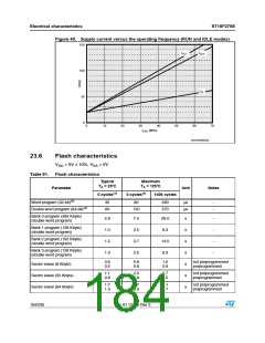
Run mode power supply current(9)
(execution from internal RAM)
ICC1
-
-
20 + 2 fCPU mA
Run mode power supply current(4)(10)
(execution from internal Flash)
ICC2
IID
-
-
-
-
20 + 1.8 fCPU mA
20 + 0.6 fCPU mA
Idle mode supply current (11)
Power Down supply current (12)
(RTC off, oscillators off, main voltage
regulator off)
IPD1
IPD2
IPD3
TA = 25°C
TA = 25°C
TA = 25°C
-
-
-
1
8
mA
mA
mA
Power Down supply current (12)
(RTC on, main oscillator on, main voltage
regulator off)
Power down supply current (12)
(RTC on, 32 kHz oscillator on, main voltage
regulator off)
1.1
VSTBY = 5.5V
TA = TJ = 25°C
-
-
-
-
-
250
500
250
500
2.5
µA
µA
µA
µA
mA
Stand-by supply current (12)
(RTC off, Oscillators off, VDD off, VSTBY on)
ISB1
VSTBY = 5.5V
TA = TJ = 125°C
VSTBY = 5.5V
TA = 25°C
Stand-by supply current (12)
(RTC on, 32 kHz Oscillator on, main VDD off,
VSTBY on)
ISB2
VSTBY = 5.5V
TA = 125°C
Stand-by supply current (4) (12)
(VDD transient condition)
ISB3
-
1. This specification is not valid for outputs which are switched to open drain mode. In this case the respective output floats
and the voltage is imposed by the external circuitry.
2. Port 5 leakage values are granted for not selected A/D converter channel. One channels is always selected (by default,
after reset, P5.0 is selected). For the selected channel the leakage value is similar to that of other port pins.
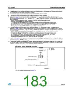
3. The leakage of P2.0 is higher than other pins due to the additional logic (pass gates active only in specific test modes)
implemented on input path. Pay attention to not stress P2.0 input pin with negative overload beyond the specified limits:
Failures in Flash reading may occur (sense amplifier perturbation). Refer to Figure 44 for a scheme of the input circuitry.
4. Not 100% tested, guaranteed by design characterization.
5. Overload conditions occur if the standard operating conditions are exceeded, that is, the voltage on any pin exceeds the
specified range (that is, V > V + 0.3V or V < -0.3V). The absolute sum of input overload currents on all port pins may
OV
DD
OV
not exceed 50mA. The supply voltage must remain within the specified limits.
182/235
Doc ID 12303 Rev 3

 STMICROELECTRONICS [ ST ]