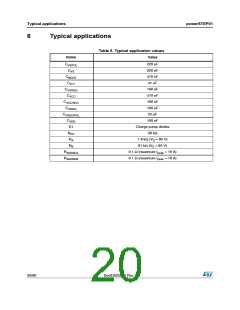
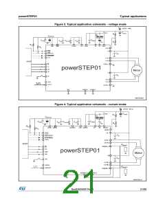
powerSTEP01
N.
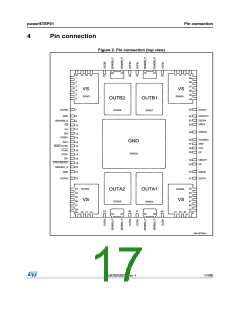
Pin list
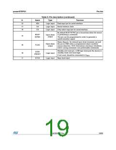
Table 5. Pin description (continued)
Type
Name
Function
12
11
10
SDI
CK
CS
Logic input
Logic input
Logic input
Data input pin for serial interface
Serial interface clock
Chip select input pin for serial interface
By default BUSY/SYNC pin is forced low when the device
is performing a command.
The pin can be programmed in order to generate a
synchronization signal.
BUSY
/SYNC
Open-drain
output
15
16
Status flag pin. An internal open-drain transistor can pull
the pin to GND when a programmed alarm condition
occurs (step loss, OCD, thermal pre-warning or shutdown,
UVLO, wrong command, non performable command).
Open-drain
output
FLAG
Standby and reset pin. LOW logic level puts the device in
standby mode and reset logic.
If not used, should be connected to VREG
STBY
/RESET
19
17
Logic input
Logic input
STCK
Step clock input
DocID025022 Rev 1
19/90

 STMICROELECTRONICS [ ST ]