Functional description
powerSTEP01
7
Functional description
7.1
Device power-up
During power-up, the device is under reset (all logic IOs disabled and power bridges in high
impedance state) until the following conditions are satisfied:
•
•
•
•
•
VCC is greater than VCCthOn
VBOOT - VS is greater than DVBOOTthOn
VREG is greater than VREGthOn
Internal oscillator is operative
STBY/RESET input is forced high.
After power-up, the device state is the following:
•
•
Parameters are set to default
Internal logic is driven by internal oscillator and a 2-MHz clock is provided by the
OSCOUT pin
•
Bridges are disabled (high impedance).
After power-up, a period of tlogicwu must pass before applying a command to allow proper
oscillator and logic startup.
Any movement command makes the device exit from High Z state (HardStop and SoftStop
included).
7.2
Logic I/O
Pins CS, CK, SDI, STCK, SW and STBY/RESET are TTL/CMOS 3.3 V to 5 V compatible
logic inputs.
Pin SDO is a TTL/CMOS compatible logic output. VDD pin voltage imposes logical output
voltage range.
Pins FLAG and BUSY/SYNC are open-drain outputs.
SW and CS inputs are internally pulled up to VDD and STBY/RESET input is internally pulled
down to ground.
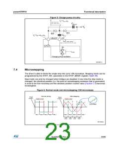
7.3
Charge pump
To ensure the correct driving of the high-side integrated MOSFETs, a voltage higher than
the motor power supply voltage needs to be applied to the VBOOT pin. The high-side gate
driver supply voltage VBOOT is obtained through an oscillator and a few external
components realizing a charge pump (see Figure 5).
22/90
DocID025022 Rev 1

 STMICROELECTRONICS [ ST ]