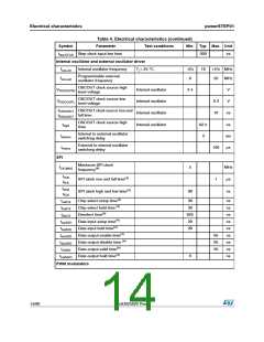
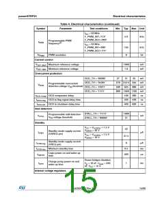
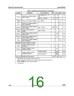
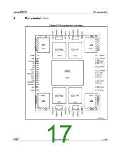
Pin list
powerSTEP01
5
Pin list
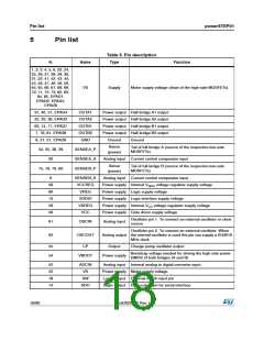
Table 5. Pin description
Type
N.
Name
Function
1, 2, 3, 4, 5, 6, 23, 24,
25, 26, 27, 28, 29, 30,
31, 32, 41, 42, 43, 44,
45, 46, 47, 48, 49, 50,
64, 65, 66, 67, 68, 69,
70, 71, 72, 73, 82, 83,
84, 85, EPAD1,
VS
Supply
Motor supply voltage (drain of the high-side MOSFETs)
EPAD2, EPAD5,
EPAD6
37, 40, 51, EPAD4
22, 33, 36, EPAD3
63, 74, 77, EPAD7
7, 78, 81, EPAD8
8, 21, 57, EPAD9
OUTA1
OUTA2
OUTB1
OUTB2
GND
Power output Half-bridge A1 output
Power output Half-bridge A2 output
Power output Half-bridge B1 output
Power output Half-bridge B2 output
Ground
Ground
Sense
(power)
Tail of full-bridge A (source of the respective low-side
MOSFETs)
34, 35, 38, 39
20
SENSEA_P
SENSEA_S
SENSEB_P
Analog input Current control comparator input
Sense
Tail of full-bridge B (source of the respective low-side
MOSFETs)
75, 76, 79, 80
(power)
9
SENSEB_S
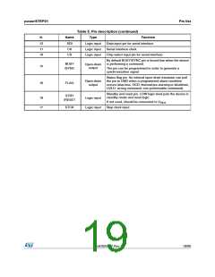
VCCREG
VREG
Analog input Current control comparator input
Power supply Internal VREG voltage regulator supply voltage
Power supply Logic supply voltage
58
60
13
59
56
VDDIO
Power supply Logic interface supply voltage
Power supply Internal VCC voltage regulator supply voltage
Power supply Gate driver supply voltage
VSREG
VCC
Oscillator pin 1. To connect an external oscillator or clock
61
62
OSCIN
Analog input
source
Oscillator pin 2. To connect an external oscillator. When
Analog output the internal oscillator is used this pin can supply a 2/4/8/16
MHz clock
OSCOUT
55
54
CP
Output
Charge pump oscillator output
Bootstrap voltage needed for driving the high-side power
DMOS of both bridges (A and B)
VBOOT
Power supply
52
53
18
14
ADCIN
VS
Analog input Internal analog to digital converter input
Power supply Motor supply voltage
SW
Logical input External switch input pin
SDO
Logic output Data output pin for serial interface
18/90
DocID025022 Rev 1

 STMICROELECTRONICS [ ST ]