Device operation
M41T00
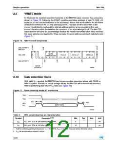
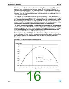
2.9
WRITE mode
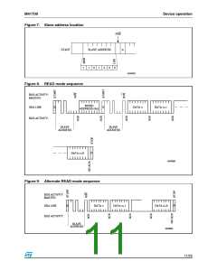
In this mode the master transmitter transmits to the M41T00 slave receiver. Bus protocol is
shown in Figure 10. Following the START condition and slave address, a logic '0' (R/W = 0)
is placed on the bus and indicates to the addressed device that word address An will follow
and is to be written to the on-chip address pointer. The data word to be written to the
memory is strobed in next and the internal address pointer is incremented to the next
memory location within the RAM on the reception of an acknowledge clock. The M41T00
slave receiver will send an acknowledge clock to the master transmitter after it has received
the slave address and again after it has received the word address and each data byte (see
Figure 7).
Figure 10. WRITE mode sequences
BUS ACTIVITY:
MASTER
WORD
ADDRESS (An)
SDA LINE
S
DATA n
DATA n+1
DATA n+X
P
BUS ACTIVITY:
SLAVE
ADDRESS
AI00591
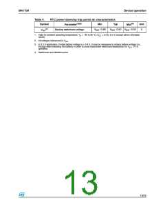
2.10
Data retention mode
With valid V applied, the M41T00 can be accessed as described above with READ or
CC
WRITE cycles. Should the supply voltage decay, the M41T00 will automatically deselect,
WRITE protecting itself when V falls (see Figure 11).
CC
Figure 11. Power down/up mode AC waveforms
V
CC
V
SO
tPD
tREC
SDA
SCL
DON'T CARE
AI00596
Table 3.
Symbol
RTC power down/up ac characteristics
Parameter(1)(2)
Min
0
Typ
Max
Unit
ns
tPD
trec
SCL and SDA at VIH before power down
SCL and SDA at VIH after power up
10
µs
1. Valid for ambient operating temperature: TA = -40 to 85°C; VCC = 2.0 to 5.5 V (except where otherwise noted).
2. VCC fall time should not exceed 5 mV/µs.
12/25

 STMICROELECTRONICS [ ST ]