L9935
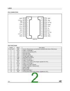
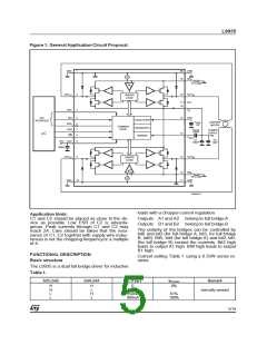
Figure 1. General Application Circuit Proposal.
GND
1
20
19
GND
~
SR
A
R1 0.33Ω
OUT
2
3
18
OUT
N.C.
A1
DRIVER
LOGIC
A2
17
16
SCK
V
S
SDI
SDO
4
5
7
8
6
15
14
OSC
SDI
INTERFACE
OSCILLATOR
DIAGNOSTIC
BIASING
C
1nF
STEPPER
MOTOR
OSC
COMMON
LOGIC
CSN
C
Driver
100nF
POWER
SUPPLY
µC
EN
C
DRV
C1
C2
10µF
+5V VCC
100nF
100nF
OUT
9
13
OUT
B1
B2
DRIVER
LOGIC
12
11
SR
B
R2 0.33Ω
GND
~
GND
10
D99AT417
loads with a choppercurrent regulation.
Application hints:
C1 and C2 should be placed as close to the de-
vice as possible. Low ESR of C2 is advanta-
geous. Peak currents through C1 and C2 may
reach 2A. Care should be taken that the reso-
nance of C1, C2 together with supply wire induc-
tances is not the chopping frequencyor a multiple
of it.
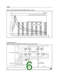
Outputs A1 and A2 belong to full bridge A
Outputs B1 and B2 belong to full bridge B
The polarity of the bridges can be controlled by
bit0 and bit3 (for full bridge A, bit3, for full bridge
B, bit0). Bit5, bit4 (for full bridge A) and bit2, bit1
(for full bridge B) control the currents. Bit3 high
leads to output A1 high. Bit0 high leads to output
B1 high.
FUNCTIONAL DESCRIPTION
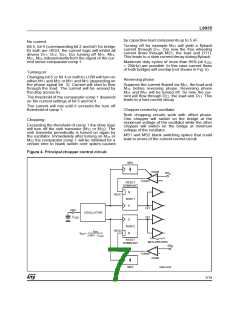
Basic structure
Current setting Table 1 using a 0.33W sense re-
sistor.
The L9935 is a dual full bridge driver for inductive
Table 1.
bit5, bit2
bit4, bit1
IQX (Typ.)
IRX/max
Remark
H
H
L
H
L
H
L
0
0%
60mA
550mA
900mA
inernally sensed
61%
100%
L
5/19

 STMICROELECTRONICS [ ST ]