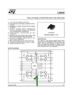
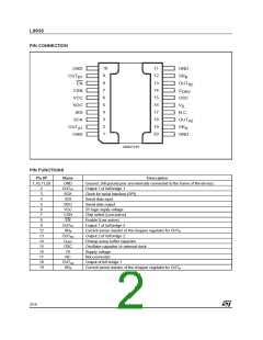
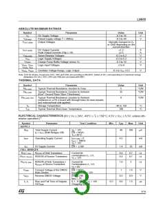
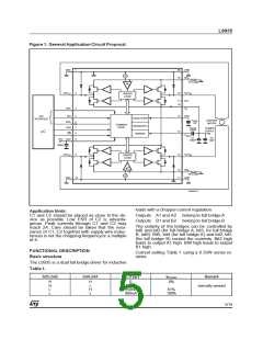
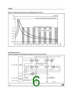
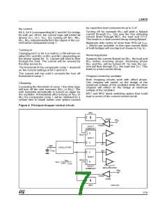
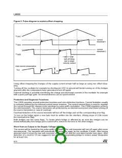
L9935
ABSOLUTE MAXIMUM RATINGS
Symbol
Parameter
Value
Unit
V
VS
DC Supply Voltage
-0.3 to 35
-0.3 to 40
VSPulsed
VOUT (Ai/Bi)
Pulsed supply voltage T < 400ms
Output Voltages
V
internally clamped to VS
or GND depending on the
current direction
IOUT (Ai/Bi)
DC Output Currents
Peak Output Currents (T/tp ≥ 10)
1.2
±2.5
A
A
±
VSRA/SRB
VCC
Sense Resistor Voltages
Logic Supply Voltages
-0.3 to 6.2
-0.3 to 6.2
-0.3 to 10
-2 to 8
V
V
V
V
VCDRV
Charge Pump Buffer Voltage versus VS
Logic Input Voltages
V
SCK, VSDI,
V
CSN, VEN
VOSC, VSDO
Oscillator Voltage Range, Logic Output
-0.3 to VCC +0.3
V
Note: ESD for all pins, except pins SDO, SRA and SRB, are according to MIL883C, tested at 2kV, corresponding to a maximum energy
dissipation of 0.2mJ. SDO, SRA and SRB pins are tested with 800V.
THERMAL DATA
Symbol
Rth j-case
Rth j-amb
Parameter
Value
5
Unit
°C/W
°C/W
Typical Thermal Resistance Junction to Case
Typical Thermal Resistance Junction to Ambient
35
(6cm2 Ground Plane 35µm Thhickness)
Rth j-amb, FR4
Typical Thermal Resistance Junction to Ambient
(soldered on a FR 4 board with through holes for heat transfer
and external heat sink applied)
8
°C/W
TS
Storage Temperature
-40 to 150
180
°C
°C
TSD
Typical Thermal Shut-Down Temperature
ELECTRICAL CHARACTERISTICS
(8V ≤ VS ≤ 24V; -40°C ≤ Tj ≤ 150°C; 4.5V ≤ VCC ≤ 5.5V, unless oth-
erwise specified.)1)
Symbol
SUPPLY
IS85
Parameter
Test Condition
Min.
Typ.
Max.
Unit
Total Supply Current
VS = 14V
40
100
A
µ
IS + IVCC (Both Bridges Off)
EN = HIGH
TJ ≤ 85°C
ISOP
Operating Supply Current
5V Supply Current
IOUT Ai/Bi = 0
4.5
1.4
mA
mA
fOSC = 30kHz
VS = 14V
ICC
FULL BRIDGES
EN = LOW
10
ROUT, Sink
RDSON of Sink Transistors
Current bit
combinations LL, LH,
0.4
0.4
0.7
0.7
Ω
Ω
ROUT, Source RDSON of Source Transistors
VS 12V
≥
ROUT8, Sink
RDSON of Sink Transistors +
DSON of Source Transistors
Current bit
Combinations LL, LH,
VS = 8V
1.6
3
Ω
R
VFWD
VREV
tr, tf
Forward Voltage of the DMOS
Body Diodes
EN = HIGH
1
1.4
0.9
1.5
V
V
I
FWD = 1A; VS ≥ 12V
EN = LOW
REV = 1A
Reverse DMOS Voltage
0.5
0.6
I
Rise and Fall Time of Outputs
OUTAi/Bi
0.1...0.9 VOUT VS = 14V
Chopping 550mA
0.3
s
µ
3/19

 STMICROELECTRONICS [ ST ]