L9935
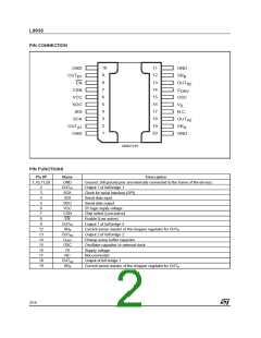
PIN CONNECTION
10
9
8
7
6
5
4
3
2
1
11
12
13
14
15
16
17
18
19
20
GND
GND
SR
OUT
B1
B
EN
OUT
B2
CSN
VCC
SDO
SDI
C
DRV
OSC
V
S
N.C.
OUT
SCK
A2
OUT
SR
A
A1
GND
GND
D99AT416
PIN FUNCTIONS
Pin No
Name
GND
Description
1,10,11,20
Ground. (All ground pins are internally connected to the frame of the device).
Output 1 of full bridge 1
2
3
OUTA1
SCK
SDI
Clock for serial interface (SPI)
Serial data input
4
5
SDO
VCC
CSN
EN
Serial data output
6
5V logic suplly voltage
7
Chip select (Low active)
8
Enable (Low active)
9
OUTB1
SRB
Output 1 of full bridge 2
12
13
14
15
16
17
18
19
Cyrrent sense resistor of the chopper regulator for OUTB
Output 2 of full bridge 2
OUTB2
CDRV
OSC
VS
Charge pump buffer capacitor
Oscillator capacitor or external clock
Supply voltage
NC
Not connected
OUTA2
SRA
Output of full bridge 1
Current sense resistor of the chopper regulator for OUTA
2/19

 STMICROELECTRONICS [ ST ]