L7250
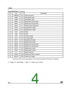
PIN DESCRIPTION (continued)
N°
44
45
46
47
48
49
50
51
52
53
54
55
56
57
58
59
60
61
62
63
64
Pin
VCMGND4
VCMN1
VCMN2
RSEN1
RSEN2
Rsense
OUTW1
OUTW2
VM1
V
Description
gnd
O12
O12
O12
O12
I5
VCM power ground
VCM negative output
VCM negative output
Spindle power sensing resitor
Spindle power sensing resitor
Spindle sensing resistor input
Spindle phase C output
Spindle phase C output
O12
O12
IO12 Vmotor
IO12 Vmotor
VM2
VCV4
S12
S12
O12
O12
O12
O12
O12
O12
I12
12V power supply
VCV3
12V power supply
OUTV1
OUTV2
RSEN3
RSEN4
OUTU1
OUTU2
CT
Spindle phase B output
Spindle phase B output
Spindle power sensing resitor
Spindle power sensing resitor
Spindle phase A output
Spindle phase A output
Spindle central tap
CPOSCH
VBOOST
IO20 Charge pump diodes connection
IO20 Charge Pump voltage
(*) used also to set the IC power supply application. If this pin is pull-up externally the L7250 became a 5V application
S = Supply ; IO = Input/Output ; I = Input ; O = Output ; gnd = Ground.
4/46

 STMICROELECTRONICS [ ST ]