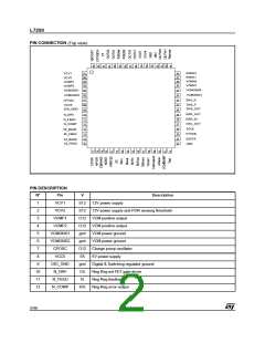
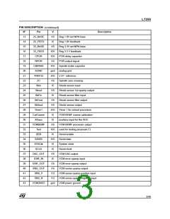
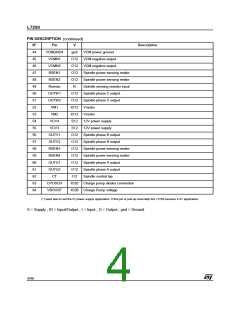
L7250
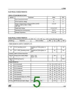
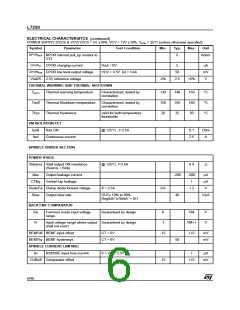
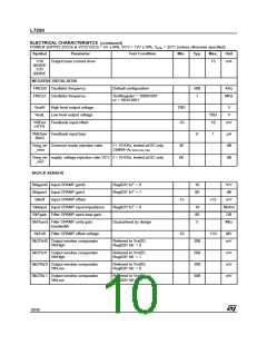
ELECTRICAL CHARACTERISTCS (continued)
POWER SUPPLY [VCC5 & VCV] VCC5 = 5V ±10%, VCV = 12V ±10%. T
= 25°C (unless otherwise specified)
amb
Symbol
Parameter
Test Condition
Min.
Typ.
Max.
Unit
NPOR
pull
NPOR internal pull_up resistor to
V33
6
Kohm
CPOR
Ic
CPOR charging current
Vout = 0V
VCV > 4.5V Iol = 1mA
5
uA
mV
V
CPOR
low
CPOR low level output voltage
50
2.5
Vref25 2.5V reference voltage
THERMAL WARNING AND THERMAL SHUTDOWN
-5%
+5%
T
Thermal warming temperature
Thermal Shutdown temperature
Thermal Hysteresis
Characterized, tested by
correlation.
130
150
20
140
165
25
150
180
30
°C
°C
°C
warn
Tsoff
Thys
Characterized, tested by
correlation
valid for both temperature
thresholds
VM ISOLATION FET
IsoR
IsoI
Rds ON
@ 125°C , I=2.5A
0.1
2.5
Ohm
A
Continuous current
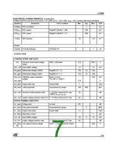
SPINDLE DRIVER SECTION
POWER STAGE
Rds(on) Total output ON resistance
(Source + Sink)
@ 125°C, I=2.5A
0.9
Ω
Idsx
Output leakage current
Centarl tap leakage
-200
40
-500
1
µA
µA
CTlkg
DiodeFw Clamp diode forward voltage
Slew Output slew rate
If = 2.5A
0.6
1.2
V
OUTx 10% to 90%
V/µS
Reg04H ‘b7b6b5’ = 011
BACK EMF COMPARATOR
Vie
Common mode input voltage
range.
Guaranteed by design
0
VM
VM+1
+15
V
V
Vr
Input voltage range where output Guaranteed by design
shall not invert.
-1
BEMFoff BEMF input offset
BEMFhy BEMF hysteresys
SPINDLE CURRENT LIMITING
CT = 6V
CT = 6V
-15
mV
mV
50
Iin
RSENSE Input bias current.
0 < Vin < 3.3V
1
µA
CURoff Comparator offset
-15
+15
mV
6/46

 STMICROELECTRONICS [ ST ]