L6599A
Application information
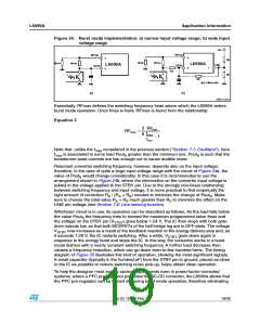
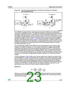
Figure 24. Burst mode implementation: a) narrow input voltage range; b) wide input
voltage range
%ꢆ
5)PLQ
67%<
5)PLQ
ꢈ
ꢉ
ꢈ
'
5
5
)PLQ
5
)PD[
5
)PLQ
5
)PD[
5
'$3ꢀꢁꢂ
/ꢅꢂꢆꢆ$
/ꢅꢂꢆꢆ$
'$3ꢀꢁꢂ
/,1(
67%<
ꢊ
ꢉ
$
5
&
%
5
$
5
%ꢄ
&
ꢃꢄ5 !!ꢄ5
Dꢎ
Eꢎ
!-ꢀꢁꢁꢆꢇVꢁ
Essentially, RFmax defines the switching frequency fmax above which the L6599A enters
burst mode operation. Once fmax is fixed, RFmax is found from the relationship:
Equation 3
3 RFmin
RFmax
=
fmax
8
−1
fmin
Note that, unlike the fmax considered in the previous section (“Section 7.1: Oscillator“), here
max is associated to some load PoutB greater than the minimum one. PoutB is such that the
f
transformer peak currents are low enough not to cause audible noise.
Resonant converter switching frequency, however, depends also on the input voltage;
therefore, in the case of quite a large input voltage range with the circuit of Figure 24a, the
value of PoutB would change considerably. In this case it is recommended to use the
arrangement shown in Figure 24b, where the information on the converter input voltage is
added to the voltage applied to the STBY pin. Due to the strongly non-linear relationship
between switching frequency and input voltage, it is more practical to find empirically the
right amount of correction RA / (RA + RB) needed to minimize the change of PoutB. Make
sure to choose the total value RA + RB much greater than RC to minimize the effect on the
LINE pin voltage (see Section 7.6: Line sensing function).
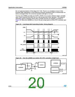
Whichever circuit is in use, its operation can be described as follows. As the load falls below
the value PoutB the frequency tries to exceed the maximum programmed value fmax and
the voltage on the STBY pin (VSTBY) goes below 1.24 V. The IC then stops with both gate-
drive outputs low, so that both MOSFETs of the half bridge leg are in OFF-state. The voltage
V
STBY now increases as a result of the feedback reaction to the energy delivery stop and, as
it exceeds 1.29 V, the IC restarts switching. After a while, VSTBY goes down again in
response to the energy burst and stops the IC. In this way, the converter works in a burst
mode fashion with a nearly constant switching frequency. A further load decrease then
causes a frequency reduction, which can go down even to few hundred hertz. The timing
diagram of Figure 25 illustrates this kind of operation, showing the most significant signals.
A small capacitor (typically in the hundred pF) from the STBY pin to ground, placed as close
to the IC as possible to reduce switching noise pick-up, helps obtain clean operation.
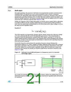
To help the designer meet energy saving requirements even in power-factor-corrected
systems, where a PFC pre-regulator precedes the DC-DC converter, the L6599A allows that
the PFC pre-regulator can be turned off during burst mode operation, therefore eliminating
Doc ID 15308 Rev 7
19/35

 STMICROELECTRONICS [ ST ]