L6599A
Application information
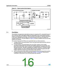
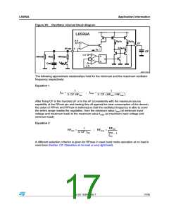
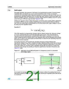
Figure 22. Oscillator internal block diagram
,ꢉꢈꢄꢄ!
ꢂ 6
ꢏ
+-q)2
+-q)2
ꢆ
#&
ꢂq+-q)2
ꢋ
2&MIN
ꢇ
)
2
#&
ꢁ 6
ꢏ
ꢋ
3
2
2&MIN
2SS
#SS
2&MAX
1
ꢏ
ꢋ
ꢇ 6
!-ꢀꢁꢁꢆꢂVꢁ
The following approximate relationships hold for the minimum and the maximum oscillator
frequency respectively:
Equation 1
1
1
fmin
=
;
fmax =
3 ⋅CF ⋅RFmin
3 ⋅CF ⋅
(
RFmin //RFmax
)
After fixing CF in the hundred pF or in the nF (consistently with the maximum source
capability of the RFmin pin and trading this off against the total consumption of the device),
the value of RFmin and RFmax is selected so that the oscillator frequency is able to cover
the entire range needed for regulation, from the minimum value fmin (at minimum input
voltage and maximum load) to the maximum value fmax (at maximum input voltage and
minimum load):
Equation 2
1
RFmin
fmax
fmin
RFmin
=
; RFmax =
3⋅CF⋅fmin
−1
A different selection criterion is given for RFmax in case burst mode operation at no load is
used (see Section 7.2: Operation at no load or very light load).
Doc ID 15308 Rev 7
17/35

 STMICROELECTRONICS [ ST ]