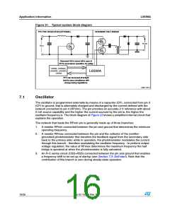
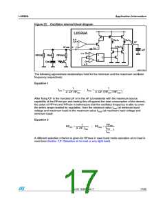
Application information
L6599A
Figure 23. Oscillator waveforms and their relationship with gate-driving signals
#&
4
$
4
$
T
T
(6'
,6'
("
T
T
!-ꢀꢁꢁꢆꢆVꢁ
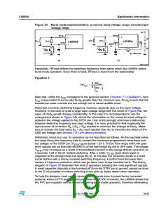
In Figure 23 the timing relationship between the oscillator waveform and the gate-drive
signal, as well as the swinging node of the half bridge leg (HB), is shown. Note that the low-
side gate drive is turned on while the oscillator triangle is ramping up and the high-side gate
drive is turned on while the triangle is ramping down. In this way, at startup, or as the IC
resumes switching during burst mode operation, the low-side MOSFET is switched on first
to charge the bootstrap capacitor. As a result, the bootstrap capacitor is always charged and
ready to supply the high-side floating driver.
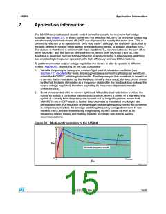
7.2
Operation at no load or very light load
When the resonant half bridge is lightly loaded or not loaded at all, its switching frequency is
at its maximum value. To keep the output voltage under control in these conditions and to
avoid losing soft-switching, there must be some significant residual current flowing through
the transformer’s magnetizing inductance. This current, however, produces some
associated losses that prevent converter no load consumption from achieving very low
values.
To overcome this issue, the L6599A enables the designer to make the converter operate
intermittently (burst mode operation), with a series of a few switching cycles spaced out by
long idle periods where both MOSFETs are in OFF-state, so that the average switching
frequency can be substantially reduced. As a result, the average value of the residual
magnetizing current and the associated losses are considerably cut down, therefore
facilitating the converter to comply with energy saving recommendations.
The L6599A can be operated in burst mode by using pin 5 (STBY): if the voltage applied to
this pin falls below 1.24 V, the IC enters an idle state where both gate-drive outputs are low,
the oscillator is stopped, the soft-start capacitor CSS keeps its charge and only the 2 V
reference at the RFmin pin stays alive to minimize IC consumption and Vcc capacitor
discharge. The IC resumes normal operation as the voltage on the pin exceeds 1.24 V by 50
mV.
To implement burst mode operation the voltage applied to the STBY pin needs to be related
to the feedback loop. Figure 24 (a) shows the simplest implementation, suitable with a
narrow input voltage range (e.g. when there is a PFC front-end).
18/35
Doc ID 15308 Rev 7

 STMICROELECTRONICS [ ST ]