Application information
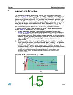
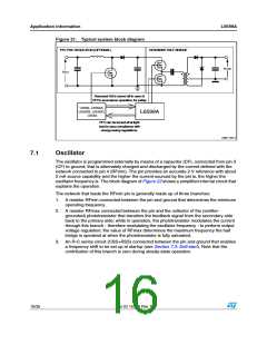
Figure 21. Typical system block diagram
L6599A
0&# 02%ꢋ2%'5,!4/2 ꢎ/04)/.!,ꢍ
2%3/.!.4 (!,&ꢋ"2)$'%
OUTDC
6
INAC
6
2ESONANT (" IS TURNED OFF IN CASE OF
0&#gS ANOMALOUS OPERATIONꢌ FOR SAFETY
,ꢉꢈꢉꢂꢌ ,ꢉꢈꢉꢂ!ꢌ
,ꢉꢈꢉꢆ3ꢌ ,ꢉꢈꢉꢆ(ꢌ
$!0ꢀꢁꢈ!
$!0ꢀꢁꢈ
,ꢉꢈꢄꢄ!
$!0ꢀꢀꢈ
,ꢉꢈꢉꢆ
,ꢉꢈꢉꢇ
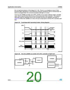
0&# CAN BE TURNED OFF AT LIGHT
LOAD TO EASE COMPLIANCE WITH
ENERGYSAVING REGULATIONSꢅ
!-ꢀꢁꢁꢆꢀVꢁ
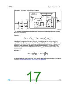
7.1
Oscillator
The oscillator is programmed externally by means of a capacitor (CF), connected from pin 3
(CF) to ground, that is alternately charged and discharged by the current defined with the
network connected to pin 4 (RFmin). The pin provides an accurate 2 V reference with about
2 mA source capability and the higher the current sourced by the pin is, the higher the
oscillator frequency is. The block diagram of Figure 22 shows a simplified internal circuit that
explains the operation.
The network that loads the RFmin pin is generally made up of three branches:
1. A resistor RFmin connected between the pin and ground that determines the minimum
operating frequency.
2. A resistor RFmax connected between the pin and the collector of the (emitter-
grounded) phototransistor that transfers the feedback signal from the secondary side
back to the primary side; while in operation, the phototransistor modulates the current
through this branch - therefore modulating the oscillator frequency - to perform output
voltage regulation; the value of RFmax determines the maximum frequency the half
bridge is operated at when the phototransistor is fully saturated.
3. An R-C series circuit (CSS+RSS) connected between the pin and ground that enables
a frequency shift to be set up at startup (see Section 7.3: Soft-start). Note that the
contribution of this branch is zero during steady-state operation.
16/35
Doc ID 15308 Rev 7

 STMICROELECTRONICS [ ST ]