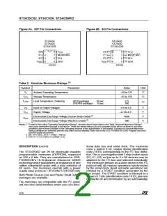
ST24/25C02, ST24C02R, ST24/25W02
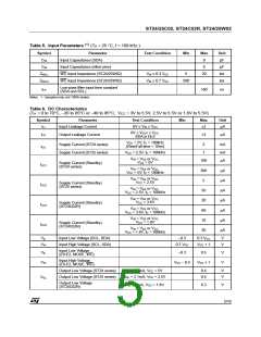
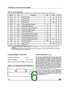
Table 7. AC Characteristics
(TA = 0 to 70°C, –20 to 85°C or –40 to 85°C; VCC = 3V to 5.5V, 2.5V to 5.5V or 1.8V to 5.5V)
Symbol
tCH1CH2
tCL1CL2
tDH1DH2
tDL1DL1
Alt
tR
Parameter
Min
Max
1
Unit
µs
ns
Clock Rise Time
Clock Fall Time
Input Rise Time
Input Fall Time
tF
300
1
tR
µs
ns
tF
300
(1)
tCHDX
tSU:STA
tHIGH
tHD:STA
tHD:DAT
tLOW
tSU:DAT
tSU:STO
tBUF
tAA
Clock High to Input Transition
Clock Pulse Width High
4.7
4
µs
µs
µs
µs
µs
ns
tCHCL
tDLCL
tCLDX
tCLCH
tDXCX
tCHDH
tDHDL
Input Low to Clock Low (START)
Clock Low to Input Transition
Clock Pulse Width Low
4
0
4.7
250
4.7
4.7
0.3
300
Input Transition to Clock Transition
Clock High to Input High (STOP)
Input High to Input Low (Bus Free)
Clock Low to Next Data Out Valid
Data Out Hold Time
µs
µs
µs
ns
(2)
tCLQV
3.5
tCLQX
fC
tDH
fSCL
tWR
Clock Frequency
100
10
kHz
ms
(3)
tW
Write Time
Notes: 1. For a reSTART condition, or following a write cycle.
2. The minimum value delays the falling/rising edge of SDA away from SCL = 1 in order to avoid unwanted START and/or STOP
conditions.
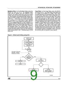
3. In the Multibyte Write mode only, if accessed bytes are on two consecutive 8 bytes rows (6 address MSB are not constant) the
maximum programming time is doubled to 20ms.
AC MEASUREMENT CONDITIONS
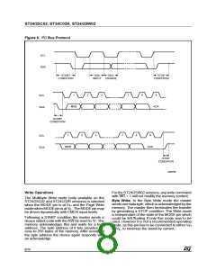
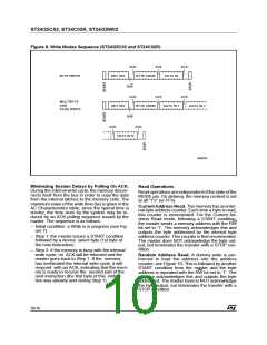
DEVICE OPERATION (cont’d)
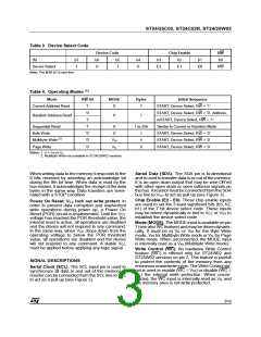
The 4 most significant bits of the device select code
are the device type identifier, corresponding to the
I2C bus definition. For these memories the 4 bits
are fixed as 1010b. The following 3 bits identify the
specific memory on the bus. They are matched to
the chip enable signals E2, E1, E0. Thus up to 8 x
2K memories can be connected on the same bus
giving a memory capacity total of 16K bits. After a
START condition any memory on the bus will iden-
tify the device code and compare the following 3
bits to its chip enable inputs E2, E1, E0.
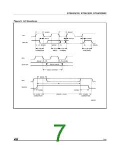
Input Rise and Fall Times
Input Pulse Voltages
≤ 50ns
0.2VCC to 0.8VCC
Input and Output Timing Ref. Voltages 0.3VCC to 0.7VCC
Figure 4. AC Testing Input Output Waveforms
0.8V
CC
0.7V
CC
The 8th bit sent is the read or write bit (RW), this
bit is set to ’1’ for read and ’0’ for write operations.
If a match is found, the corresponding memory will
acknowledge the identification on the SDA bus
during the 9th bit time.
0.3V
CC
0.2V
CC
AI00825
6/16

 STMICROELECTRONICS [ ST ]