ST24/25C02, ST24C02R, ST24/25W02
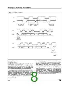
Multibyte Write. For the Multibyte Write mode, the
MODE pin must be at VIH. The Multibyte Write
mode can be started from any address in the
memory. The master sends from one up to 4 bytes
of data, whichare eachacknowledgedbythemem-
ory. The transfer is terminated by the master gen-
erating a STOP condition. The duration of the write
cycle is tW = 10ms maximum except when bytes
are accessed on 2 rows (that is have different
values for the 6 most significant address bits A7-
A2), the programming time is then doubled to a
maximum of 20ms. Writing more than 4bytes in the
Multibyte Write mode may modify data bytes in an
adjacent row (one row is 8 bytes long). However,
the Multibyte Write can properly write up to 8
consecutive bytes only if the first address of these
8bytesisthefirst address ofthe row, the7 following
bytes being written in the 7 following bytes of this
same row.
Page Write. For the Page Write mode, the MODE
pin must be at VIL. The Page Write mode allows up
to 8 bytes to be written in a single write cycle,
provided that they are all located in the same ’row’
in the memory: that is the 5 most significant mem-
ory address bits (A7-A3) are the same. The master
sends from one up to 8 bytes of data, which are
each acknowledged by the memory. After each
byteis transfered,theinternalbyte addresscounter
(3 least significant bits only) is incremented. The
transfer is terminated by the master generating a
STOP condition. Care must be taken to avoid ad-
dress counter ’roll-over’ which could result in data
being overwritten. Note that, for any write mode,
the generationby the masterof the STOP condition
starts the internal memory programcycle. All inputs
are disabled until the completion of this cycle and
the memory will not respond to any request.
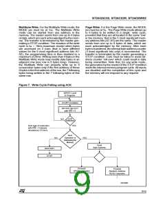
Figure 7. Write Cycle Polling using ACK
WRITE Cycle
in Progress
START Condition
DEVICE SELECT
with RW = 0
ACK
Returned
NO
First byte of instruction
with RW = 0 already
decoded by ST24xxx
YES
Next
Operation is
Addressing the
Memory
NO
YES
Send
Byte Address
ReSTART
STOP
Proceed
WRITE Operation
Proceed
Random Address
READ Operation
AI01099B
9/16

 STMICROELECTRONICS [ ST ]