ST24/25C02, ST24C02R, ST24/25W02
Table 3. Device Select Code
Device Code
Chip Enable
RW
b0
Bit
b7
1
b6
b5
1
b4
0
b3
b2
b1
Device Select
0
E2
E1
E0
RW
Note: The MSB b7 is sent first.
Table 4. Operating Modes (1)
Mode
RW bit
MODE
Bytes
Initial Sequence
START, Device Select, RW = ’1’
Current Address Read
’1’
’0’
’1’
’1’
’0’
’0’
’0’
X
1
START, Device Select, RW = ’0’, Address,
reSTART, Device Select, RW = ’1’
Similar to Current or Random Mode
START, Device Select, RW = ’0’
START, Device Select, RW = ’0’
START, Device Select, RW = ’0’
Random Address Read
X
1
Sequential Read
Byte Write
X
X
1 to 256
1
4
8
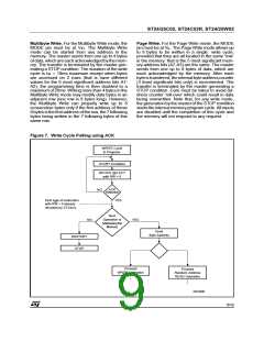
Multibyte Write (2)
VIH
VIL
Page Write
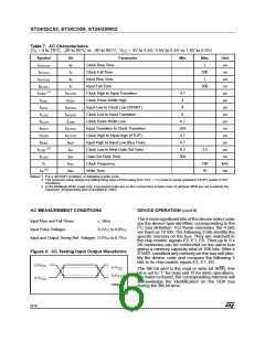
Notes: 1. X = VIH or VIL
2. Multibyte Write not available in ST24/25W02 versions.
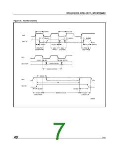
When writing data to the memory it responds to the
8 bits received by asserting an acknowledge bit
during the 9th bit time. When data is read by the
bus master, it acknowledges the receipt of the data
bytes in the same way. Data transfers are termi-
nated with a STOP condition.
Serial Data (SDA). The SDA pin is bi-directional
and is used to transfer data in or out of the memory.
It is an open drain output that may be wire-OR’ed
with other open drain or open collector signals on
thebus. Aresistormust beconnectedfromtheSDA
bus line to VCC to act as pull up (see Figure 3).
Chip Enable (E2 - E0). These chip enable inputs
are used to set the 3 least significant bits (b3, b2,
b1) of the 7 bit device select code. These inputs
may be driven dynamically or tied to VCC or VSS to
establish the device select code.
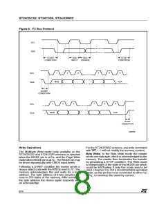
Mode (MODE). The MODE input is available on pin
7 (see also WC feature) and may bedrivendynami-
cally. It must be at VIL or VIH for the Byte Write
mode, VIH for Multibyte Write mode or VIL for Page
Write mode. When unconnected, the MODE input
is internally read as a VIH (Multibyte Write mode).
Write Control (WC). An hardware Write Control
feature (WC) is offered only for ST24W02 and
ST25W02 versions on pin 7. This feature is usefull
to protect the contents of the memory from any
erroneous erase/write cycle. The Write Control sig-
nal is used to enable (WC = VIH) or disable (WC =
VIL) the internal write protection. When uncon-
nected, the WC input is internally read as VIL and
the memory area is not write protected.
Power On Reset: VCC lock out write protect. In
order to prevent data corruption and inadvertent
write operations during power up, a Power On
Reset (POR) circuit is implemented. Until the VCC
voltage has reached the POR threshold value, the
internal reset is active, all operations are disabled
and the device will not respond to any command.
In the same way, when VCC drops down from the
operating voltage to below the POR threshold
value, all operations are disabled and the device
will not respond to any command. A stable VCC
must be applied before applying any logic signal.
SIGNAL DESCRIPTIONS
Serial Clock (SCL). The SCL input pin is used to
synchronize all data in and out of the memory. A
resistor can be connected from the SCL line to VCC
to act as a pull up (see Figure 3).
3/16

 STMICROELECTRONICS [ ST ]