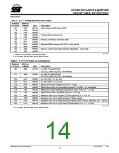
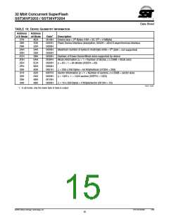
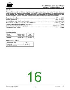
32 Mbit Concurrent SuperFlash
SST36VF3203 / SST36VF3204
Data Sheet
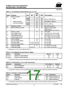
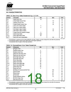
AC CHARACTERISTICS
TABLE 15: READ CYCLE TIMING PARAMETERS VDD = 2.7-3.6V
Symbol
TRC
Parameter
Min
Max
Units
ns
Read Cycle Time
70
TCE
Chip Enable Access Time
Address Access Time
70
70
35
ns
TAA
ns
TOE
Output Enable Access Time
CE# Low to Active Output
OE# Low to Active Output
CE# High to High-Z Output
OE# High to High-Z Output
Output Hold from Address Change
RST# Pulse Width
ns
1
TCLZ
0
0
ns
1
TOLZ
ns
1
TCHZ
16
16
ns
1
TOHZ
ns
1
TOH
0
ns
1
TRP
500
50
ns
1
TRHR
RST# High before Read
RST# Pin Low to Read Mode
ns
1,2
TRY
20
µs
T15.1 1270
1. This parameter is measured only for initial qualification and after a design or process change that could affect this parameter.
2. This parameter applies to Sector-Erase, Block-Erase, and Program operations.
This parameter does not apply to Chip-Erase operations.
TABLE 16: PROGRAM/ERASE CYCLE TIMING PARAMETERS
Symbol
TBP
Parameter
Min
Max
Units
µs
Program Time
10
TAS
Address Setup Time
Address Hold Time
WE# and CE# Setup Time
WE# and CE# Hold Time
OE# High Setup Time
OE# High Hold Time
CE# Pulse Width
0
40
0
ns
TAH
ns
TCS
ns
TCH
0
ns
TOES
TOEH
TCP
0
ns
10
40
40
30
30
30
0
ns
ns
TWP
WE# Pulse Width
ns
1
TWPH
WE# Pulse Width High
CE# Pulse Width High
Data Setup Time
ns
1
TCPH
ns
TDS
ns
1
TDH
Data Hold Time
ns
1
TIDA
Software ID Access and Exit Time
Sector-Erase
150
25
25
ns
TSE
TBE
TSCE
TES
ms
ms
ms
µs
Block-Erase
Chip-Erase
50
Erase-Suspend Latency
RY/BY# Delay Time
Bus Recovery Time
10
1,2
TBY
90
ns
1
TBR
0
µs
T16.1 1270
1. This parameter is measured only for initial qualification and after a design or process change that could affect this parameter.
2. This parameter applies to Sector-Erase, Block-Erase, and Program operations.
This parameter does not apply to Chip-Erase operations.
©2005 Silicon Storage Technology, Inc.
S71270-03-000
7/06
18

 SST [ SILICON STORAGE TECHNOLOGY, INC ]