32 Mbit Concurrent SuperFlash
SST36VF3203 / SST36VF3204
Data Sheet
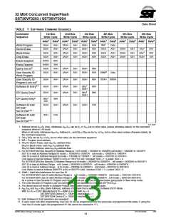
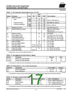
TABLE 11: DC OPERATING CHARACTERISTICS VDD = 2.7-3.6V
Limits
Symbol Parameter
Freq
Min
Max
Units
Test Conditions
1
IDD
Active VDD Current
Read
5 MHz
1 MHz
15
4
mA
mA
mA
mA
mA
µA
CE#=VIL, WE#=OE#=VIH
CE#=WE#=VIL, OE#=VIH
CE#=VIL, OE#=VIH
Program and Erase
30
45
35
20
20
Concurrent Read/Write
5 MHz
1 MHz
ISB
Standby VDD Current
CE#, RST#=VDD 0.3V
IALP
Auto Low Power VDD Current
µA
CE#=0.1V, VDD=VDD Max
WE#=VDD-0.1V
Address inputs=0.1V or VDD-0.1V
IRT
ILI
Reset VDD Current
20
1
µA
µA
µA
RST#=GND
Input Leakage Current
VIN =GND to VDD, VDD=VDD Max
ILIW
Input Leakage Current
on WP# pin and RST# pin
10
WP#=GND to VDD, VDD=VDD Max
RST#=GND to VDD, VDD=VDD Max
ILO
Output Leakage Current
Input Low Voltage
1
µA
V
VOUT =GND to VDD, VDD=VDD Max
VDD=VDD Min
VIL
0.8
0.3
VILC
VIH
Input Low Voltage (CMOS)
Input High Voltage
V
VDD=VDD Max
0.7 VDD VDD+0.3
VDD-0.3 VDD+0.3
0.2
V
VDD=VDD Max
VIHC
VOL
VOH
Input High Voltage (CMOS)
Output Low Voltage
V
VDD=VDD Max
V
IOL=100 µA, VDD=VDD Min
IOH=-100 µA, VDD=VDD Min
Output High Voltage
VDD-0.2
V
T11.1 1270
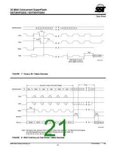
1. Address input = VILT/VIHT, VDD=VDD Max (See Figure 17)
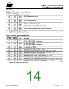
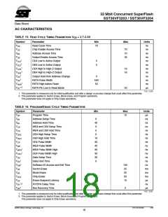
TABLE 12: RECOMMENDED SYSTEM POWER-UP TIMINGS
Symbol
Parameter
Minimum
100
Units
1
TPU-READ
Power-up to Read Operation
Power-up to Write Operation
µs
µs
1
TPU-WRITE
100
T12.0 1270
1. This parameter is measured only for initial qualification and after a design or process change that could affect this parameter.
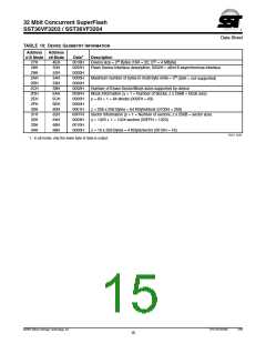
TABLE 13: CAPACITANCE (TA = 25°C, f=1 Mhz, other pins open)
Parameter
Description
Test Condition
VI/O = 0V
Maximum
1
CI/O
I/O Pin Capacitance
Input Capacitance
10 pF
10 pF
1
CIN
VIN = 0V
T13.0 1270
1. This parameter is measured only for initial qualification and after a design or process change that could affect this parameter.
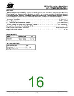
TABLE 14: RELIABILITY CHARACTERISTICS
Symbol
Parameter
Endurance
Data Retention
Latch Up
Minimum Specification
Units
Test Method
1
NEND
10,000
100
Cycles JEDEC Standard A117
1
TDR
Years
mA
JEDEC Standard A103
JEDEC Standard 78
1
ILTH
100 + IDD
T14.0 1270
1. This parameter is measured only for initial qualification and after a design or process change that could affect this parameter.
©2005 Silicon Storage Technology, Inc.
S71270-03-000
7/06
17

 SST [ SILICON STORAGE TECHNOLOGY, INC ]