32 Mbit Concurrent SuperFlash
SST36VF3203 / SST36VF3204
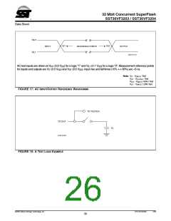
Data Sheet
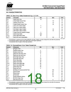
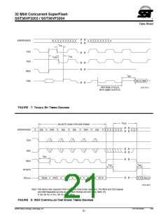
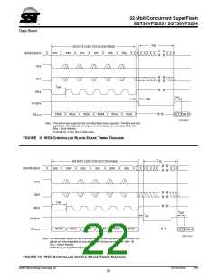
T
BE
SIX-BYTE CODE FOR BLOCK-ERASE
555 555 2AA
555
2AA
BA
ADDRESSES
X
CE#
OE#
T
WP
WE#
T
BR
T
BY
RY/BY#
VALID
XXAA
XX55
XX80
XXAA
XX55
XX30
DQ
15-0
1270 F09.0
Note: This device also supports CE# controlled Block-Erase operation. The WE# and CE#
signals are interchageable as long as minimum timings are met. (See Table 16)
BA = Block Address
X
X can be V or V , but no other value.
IL IH
FIGURE 9: WE# CONTROLLED BLOCK-ERASE TIMING DIAGRAM
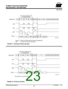
T
SE
SIX-BYTE CODE FOR SECTOR-ERASE
555
2AA
555
555
2AA
SA
ADDRESSES
X
CE#
OE#
T
WP
WE#
T
BR
T
BY
RY/BY#
XXAA
XX55
XX80
XXAA
XX55
XX50
DQ
VALID
15-0
1270 F10.0
Note: This device also supports CE# controlled Sector-Erase operation. The WE# and CE#
signals are interchageable as long as minimum timings are met. (See Table 16)
SA = Sector Address
X
X can be V or V but no other value.
IL IH,
FIGURE 10: WE# CONTROLLED SECTOR-ERASE TIMING DIAGRAM
©2005 Silicon Storage Technology, Inc.
S71270-03-000
7/06
22

 SST [ SILICON STORAGE TECHNOLOGY, INC ]