PDF
最近搜索
热门搜索
发布采购

| 型号: | S71GL064A80BAI0F3 |
| PDF下载: | 下载PDF文件 查看货源 |
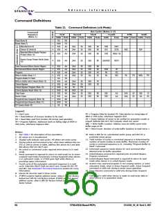
| 内容描述: | 堆叠式多芯片产品( MCP )闪存和RAM [Stacked Multi-Chip Product (MCP) Flash Memory and RAM] |
| 分类和应用: | 闪存 |
| 文件页数/大小: | 102 页 / 1762 K |
| 品牌: |  SPANSION [ SPANSION ] SPANSION [ SPANSION ] |
专业IC领域供求交易平台:提供全面的IC Datasheet资料和资讯,Datasheet 1000万数据,IC品牌1000多家。