A d v a n c e I n f o r m a t i o n
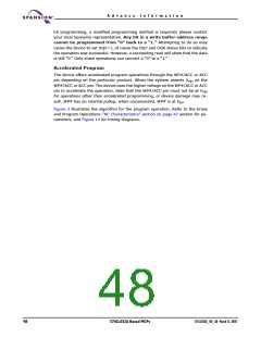
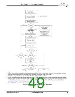
Write “Write to Buffer”
command and
Sector Address
Part of “Write to Buffer”
Command Sequence
Write number of addresses
to program minus 1(WC)
and Sector Address
Write first address/data
Yes
WC = 0 ?
No
Write to a different
sector address
Abort Write to
Buffer Operation?
Yes
Write to buffer ABORTED.
Must write “Write-to-buffer
Abort Reset” command
sequence to return
No
Write next address/data pair
(Note 1)
to read mode.
WC = WC - 1
Write program buffer to
flash sector address
Read DQ7 - DQ0 at
Last Loaded Address
Yes
DQ7 = Data?
No
No
No
DQ1 = 1?
DQ5 = 1?
Yes
Yes
Read DQ7 - DQ0 with
address = Last Loaded
Address
Yes
(Note 2)
DQ7 = Data?
No
FAIL or ABORT
PASS
(Note 3)
Notes:
1. When Sector Address is specified, any address in the selected sector is acceptable. However, when loading Write-Buffer
address locations with data, all addresses must fall within the selected Write-Buffer Page.
2. DQ7 may change simultaneously with DQ5. Therefore, DQ7 should be verified.
3. If this flowchart location was reached because DQ5= “1”, then the device FAILED. If this flowchart location was reached
because DQ1= “1”, then the Write to Buffer operation was ABORTED. In either case, the proper reset command must be
written before the device can begin another operation. If DQ1=1, write the Write-Buffer-Programming-Abort-Reset
command. if DQ5=1, write the Reset command.
4. See Table 22 for command sequences required for write buffer programming.
Figure 3. Write Buffer Programming Operation
March 31, 2005 S71GL032A_00_A0
S71GL032A Based MCPs
49

 SPANSION [ SPANSION ]