A d v a n c e I n f o r m a t i o n
Command Definitions
Table 22. Command Definitions (x16 Mode)
Bus Cycles (Notes 2–5)
Command
Sequence
(Note 1)
First
Second
Third
Fourth
Fifth
Sixth
Addr Data
Addr
Data
Addr
Data
Addr
Data
Addr Data Addr Data
Read (Note 6)
1
1
4
4
RA
XXX
555
555
RD
F0
Reset (Note 7)
Manufacturer ID
Device ID (Note 9)
AA
AA
2AA
2AA
55
55
555
555
90
90
X00
X01
0001
227E
X0E
X0F
Secured SiliconSector Factory
Protect (Note 10)
4
555
AA
2AA
55
555
90
X03
(Note 10)
Sector Group Protect Verify (Note
12)
4
555
AA
2AA
55
555
90
(SA)X02
00/01
Enter Secured Silicon Sector Region
Exit Secured Silicon Sector Region
Program
3
4
4
3
1
3
3
2
2
6
6
1
1
1
555
555
555
555
SA
AA
AA
AA
AA
29
2AA
2AA
2AA
2AA
55
55
55
55
555
555
555
SA
88
90
A0
25
XXX
PA
00
PD
WC
Write to Buffer (Note 11)
Program Buffer to Flash
Write to Buffer Abort Reset (Note 13)
Unlock Bypass
SA
PA
PD
WBL
PD
555
555
XXX
XXX
555
555
XXX
XXX
55
AA
AA
A0
90
2AA
2AA
PA
55
55
PD
00
55
55
555
555
F0
20
Unlock Bypass Program (Note 14)
Unlock Bypass Reset (Note 15)
Chip Erase
XXX
2AA
2AA
AA
AA
B0
30
555
555
80
80
555
555
AA
AA
2AA
2AA
55
55
555
SA
10
30
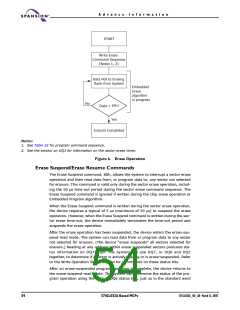
Sector Erase
Program/Erase Suspend (Note 16)
Program/Erase Resume (Note 17)
CFI Query (Note 18)
98
Legend:
X = Don’t care
RA = Read Address of memory location to be read.
PD = Program Data for location PA. Data latches on rising edge of
WE# or CE# pulse, whichever happens first.
SA = Sector Address of sector to be verified (in autoselect mode) or
erased. Address bits A21–A15 uniquely select any sector.
WBL = Write Buffer Location. Address must be within same write
buffer page as PA.
RD = Read Data read from location RA during read operation.
PA = Program Address. Addresses latch on falling edge of WE# or
CE# pulse, whichever happens later.
WC = Word Count. Number of write buffer locations to load minus 1.
Notes:
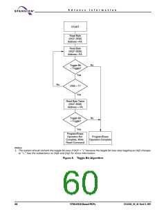
1. See Table 1 for description of bus operations.
2. All values are in hexadecimal.
10. Data is 00h for an unprotected sector group and 01h for a
protected sector group.
11. Total number of cycles in command sequence is determined by
number of words written to write buffer. Maximum number of
cycles in command sequence is 21, including “Program Buffer to
Flash” command.
12. Command sequence resets device for next command after
aborted write-to-buffer operation.
3. Shaded cells indicate read cycles. All others are write cycles.
4. During unlock and command cycles, when lower address bits are
555 or 2AA as shown in table, address bits above A11 and data
bits above DQ7 are don’t care.
5. No unlock or command cycles required when device is in read
mode.
6. Reset command is required to return to read mode (or to erase-
suspend-read mode if previously in Erase Suspend) when device
is in autoselect mode, or if DQ5 goes high while device is
providing status information.
7. Fourth cycle of the autoselect command sequence is a read
cycle. Data bits DQ15–DQ8 are don’t care. Except for RD, PD
and WC. See Autoselect Command Sequence section for more
information.
13. Unlock Bypass command is required prior to Unlock Bypass
Program command.
14. Unlock Bypass Reset command is required to return to read
mode when device is in unlock bypass mode.
15. System may read and program in non-erasing sectors, or enter
autoselect mode, when in Erase Suspend mode. Erase Suspend
command is valid only during a sector erase operation.
16. Erase Resume command is valid only during Erase Suspend
mode.
8. Device ID must be read in three cycles.
17. Command is valid when device is ready to read array data or
when device is in autoselect mode.
9. If WP# protects highest address sector, data is 98h for factory
locked and 18h for not factory locked. If WP# protects lowest
address sector, data is 88h for factory locked and 08h for not
factor locked.
56
S71GL032A Based MCPs
S71GL032A_00_A0 March 31, 2005

 SPANSION [ SPANSION ]