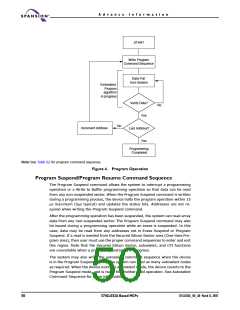
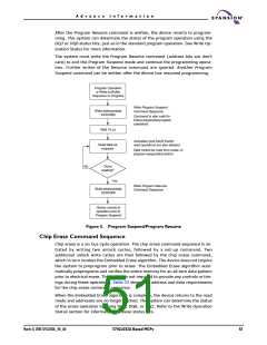
A d v a n c e I n f o r m a t i o n
bit programming, a modified programming method is required; please contact
your local Spansion representative. Any bit in a write buffer address range
cannot be programmed from “0” back to a “1.” Attempting to do so may
cause the device to set DQ5=1, of cause the DQ7 and DQ6 status bits to indicate
the operation was successful. However, a succeeding read will show that the data
is still “0.” Only erase operations can convert a “0” to a “1.”
Accelerated Program
The device offers accelerated program operations through the WP#/ACC or ACC
pin depending on the particular product. When the system asserts VHH on the
WP#/ACC or ACC pin. The device uses the higher voltage on the WP#/ACC or ACC
pin to accelerate the operation. Note that the WP#/ACC pin must not be at VHH
for operations other than accelerated programming, or device damage may re-
sult. WP# has an internal pullup; when unconnected, WP# is at VIH
.
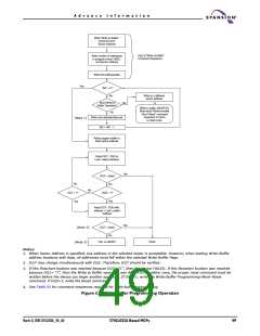
Figure 3 illustrates the algorithm for the program operation. Refer to the Erase
and Program Operations–“AC Characteristics” section on page 67 section for pa-
rameters, and Figure 14 for timing diagrams.
48
S71GL032A Based MCPs
S71GL032A_00_A0 March 31, 2005

 SPANSION [ SPANSION ]