A d v a n c e I n f o r m a t i o n
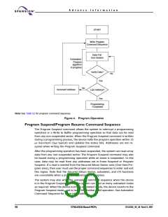
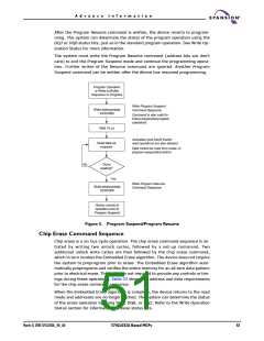
After the Program Resume command is written, the device reverts to program-
ming. The system can determine the status of the program operation using the
DQ7 or DQ6 status bits, just as in the standard program operation. See Write Op-
eration Status for more information.
The system must write the Program Resume command (address bits are don’t
care) to exit the Program Suspend mode and continue the programming opera-
tion. Further writes of the Resume command are ignored. Another Program
Suspend command can be written after the device has resumed programming.
Program Operation
or Write-to-Buffer
Sequence in Progress
Write Program Suspend
Command Sequence
Write address/data
XXXh/B0h
Command is also valid for
Erase-suspended-program
operations
Wait 15 µs
Autoselect and SecSi Sector
read operations are also allowed
Read data as
required
Data cannot be read from erase- or
program-suspended sectors
Done
No
reading?
Yes
Write Program Resume
Command Sequence
Write address/data
XXXh/30h
Device reverts to
operation prior to
Program Suspend
Figure 5. Program Suspend/Program Resume
Chip Erase Command Sequence
Chip erase is a six bus cycle operation. The chip erase command sequence is ini-
tiated by writing two unlock cycles, followed by a set-up command. Two
additional unlock write cycles are then followed by the chip erase command,
which in turn invokes the Embedded Erase algorithm. The device does not require
the system to preprogram prior to erase. The Embedded Erase algorithm auto-
matically preprograms and verifies the entire memory for an all zero data pattern
prior to electrical erase. The system is not required to provide any controls or tim-
ings during these operations. Table 22 shows the address and data requirements
for the chip erase command sequence.
When the Embedded Erase algorithm is complete, the device returns to the read
mode and addresses are no longer latched. The system can determine the status
of the erase operation by using DQ7, DQ6, or DQ2. Refer to the Write Operation
Status section for information on these status bits.
March 31, 2005 S71GL032A_00_A0
S71GL032A Based MCPs
51

 SPANSION [ SPANSION ]