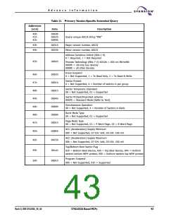
A d v a n c e I n f o r m a t i o n
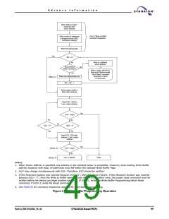
if the system will program 6 unique address locations, then 05h should be written
to the device. This tells the device how many write buffer addresses will be loaded
with data and therefore when to expect the Program Buffer to Flash command.
The number of locations to program cannot exceed the size of the write buffer or
the operation will abort.
The fifth cycle writes the first address location and data to be programmed. The
write-buffer-page is selected by address bits AMAX–A4. All subsequent address/
data pairs must fall within the selected-write-buffer-page. The system then
writes the remaining address/data pairs into the write buffer. Write buffer loca-
tions may be loaded in any order.
The write-buffer-page address must be the same for all address/data pairs loaded
into the write buffer. (This means Write Buffer Programming cannot be performed
across multiple write-buffer pages.) This also means that Write Buffer Program-
ming cannot be performed across multiple sectors. If the system attempts to load
programming data outside of the selected write-buffer page, the operation will
abort.
Note that if a Write Buffer address location is loaded multiple times, the address/
data pair counter will be decremented for every data load operation. The host
system must therefore account for loading a write-buffer location more than
once. The counter decrements for each data load operation, not for each unique
write-buffer-address location. Note also that if an address location is loaded more
than once into the buffer, the final data loaded for that address will be
programmed.
Once the specified number of write buffer locations have been loaded, the system
must then write the Program Buffer to Flash command at the sector address. Any
other address and data combination aborts the Write Buffer Programming oper-
ation. The device then begins programming. Data polling should be used while
monitoring the last address location loaded into the write buffer. DQ7, DQ6, DQ5,
and DQ1 should be monitored to determine the device status during Write Buffer
Programming.
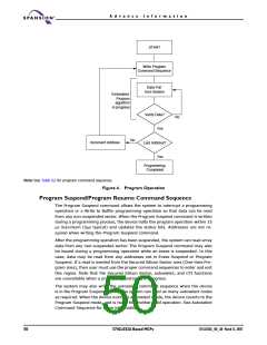
The write-buffer programming operation can be suspended using the standard
program suspend/resume commands. Upon successful completion of the Write
Buffer Programming operation, the device is ready to execute the next command.
The Write Buffer Programming Sequence can be aborted in the following ways:
Load a value that is greater than the page buffer size during the Number of
Locations to Program step.
Write to an address in a sector different than the one specified during the
Write-Buffer-Load command.
Write an Address/Data pair to a different write-buffer-page than the one se-
lected by the Starting Address during the write buffer data loading stage of
the operation.
Write data other than the Confirm Command after the specified number of
data load cycles.
The abort condition is indicated by DQ1 = 1, DQ7 = DATA# (for the last address
location loaded), DQ6 = toggle, and DQ5=0. A Write-to-Buffer-Abort Reset com-
mand sequence must be written to reset the device for the next operation.
Note that the Secured Silicon Sector, autoselect, and CFI functions are unavail-
able when a program operation is in progress.This flash device is capable of
handling multiple write buffer programming operations on the same write buffer
address range without intervening erases. For applications requiring incremental
March 31, 2005 S71GL032A_00_A0
S71GL032A Based MCPs
47

 SPANSION [ SPANSION ]