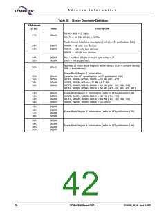
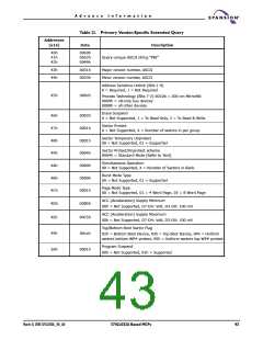
A d v a n c e I n f o r m a t i o n
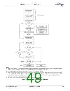
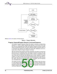
When the Embedded Program algorithm is complete, the device then returns to
the read mode and addresses are no longer latched. The system can determine
the status of the program operation by using DQ7 or DQ6. Refer to the Write Op-
eration Status section for information on these status bits. Any commands
written to the device during the Embedded Program Algorithm are ignored. Note
that the Secured Silicon Sector, autoselect, and CFI functions are unavailable
when a program operation is in progress. Note that a hardware reset immedi-
ately terminates the program operation. The program command sequence should
be reinitiated once the device has returned to the read mode, to ensure data
integrity.
Programming is allowed in any sequence of address locations and across sector
boundaries. Programming to the same word address multiple times without in-
tervening erases (incremental bit programming) requires a modified
programming method. For such application requirements, please contact your
local Spansion representative. Word programming is supported for backward
compatibility with existing Flash driver software and for occasional writing of in-
dividual words. Use of write buffer programming (see below) is strongly
recommended for general programming use when more than a few words are to
be programmed. The effective word programming time using write buffer pro-
gramming is approximately four times shorter than the single word programming
time.
Any bit in a word cannot be programmed from “0” back to a “1.” Attempt-
ing to do so may cause the device to set DQ5=1, or cause DQ7 and DQ6 status
bits to indicate the operation was successful. However, a succeeding read will
show that the data is still “0.” Only erase operations can convert a “0” to a “1.”
Unlock Bypass Command Sequence
The unlock bypass feature allows the system to program words to the device
faster than using the standard program command sequence. The unlock bypass
command sequence is initiated by first writing two unlock cycles. This is followed
by a third write cycle containing the unlock bypass command, 20h. The device
then enters the unlock bypass mode. A two-cycle unlock bypass mode command
sequence is all that is required to program in this mode. The first cycle in this se-
quence contains the unlock bypass program command, A0h; the second cycle
contains the program address and data. Additional data is programmed in the
same manner. This mode dispenses with the initial two unlock cycles required in
the standard program command sequence, resulting in faster total programming
time.Table 22 shows the requirements for the command sequence.
During the unlock bypass mode, only the Unlock Bypass Program and Unlock By-
pass Reset commands are valid. To exit the unlock bypass mode, the system
must issue the two-cycle unlock bypass reset command sequence. The first cycle
must contain the data 90h. The second cycle must contain the data 00h. The de-
vice then returns to the read mode.
Write Buffer Programming
Write Buffer Programming allows the system write to a maximum of 16 in one
programming operation. This results in faster effective programming time than
the standard programming algorithms. The Write Buffer Programming command
sequence is initiated by first writing two unlock cycles. This is followed by a third
write cycle containing the Write Buffer Load command written at the Sector Ad-
dress in which programming will occur. The fourth cycle writes the sector address
and the number of word locations, minus one, to be programmed. For example,
46
S71GL032A Based MCPs
S71GL032A_00_A0 March 31, 2005

 SPANSION [ SPANSION ]