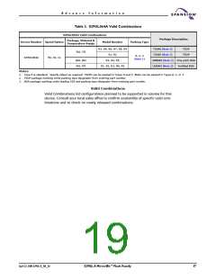
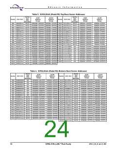
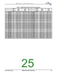
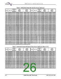
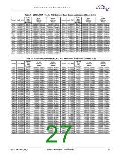
A d v a n c e I n f o r m a t i o n
Automatic Sleep Mode
The automatic sleep mode minimizes Flash device energy consumption. The de-
vice automatically enables this mode when addresses remain stable for t
+
ACC
30 ns. The automatic sleep mode is independent of the CE#, WE#, and OE# con-
trol signals. Standard address access timings provide new data when addresses
are changed. While in sleep mode, output data is latched and always available
to the system. Refer to the DC Characteristics on page 64 for the automatic
sleep mode current specification.
RESET#: Hardware Reset Pin
The RESET# pin provides a hardware method of resetting the device to reading
array data. When the RESET# pin is driven low for at least a period of t , the
RP
device immediately terminates any operation in progress, tristates all output
pins, and ignores all read/write commands for the duration of the RESET# pulse.
The device also resets the internal state machine to reading array data. The op-
eration that was interrupted should be reinitiated once the device is ready to
accept another command sequence, to ensure data integrity.
Current is reduced for the duration of the RESET# pulse. When RESET# is held
at V ±0.3 V, the device draws CMOS standby current (I
). If RESET# is held
CC5
SS
at V but not within V ±0.3 V, the standby current is greater.
IL
SS
The RESET# pin may be tied to the system reset circuitry. A system reset would
thus also reset the Flash memory, enabling the system to read the boot-up firm-
ware from the Flash memory.
Refer to the AC Characteristics tables for RESET# parameters and to Figure 15,
on page 69 for the timing diagram.
Output Disable Mode
When the OE# input is at V , output from the device is disabled. The output
IH
pins are placed in the high impedance state.
April 22, 2005 S29GL-A_00_A3
S29GL-A MirrorBit™ Flash Family
21

 SPANSION [ SPANSION ]