A d v a n c e I n f o r m a t i o n
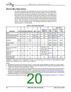
Device Bus Operations
This section describes the requirements and use of the device bus operations,
which are initiated through the internal command register. The command regis-
ter itself does not occupy any addressable memory location. The register is a
latch used to store the commands, along with the address and data information
needed to execute the command. The contents of the register serve as inputs to
the internal state machine. The state machine outputs dictate the function of the
device. Table 4 lists the device bus operations, the inputs and control levels they
require, and the resulting output. The following subsections describe each of
these operations in further detail.
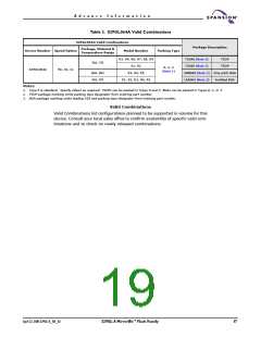
Table 4. Device Bus Operations
DQ8–DQ15
BYTE# BYTE#
Addresses
(Note 1)
DQ0–
DQ7
Operation
CE# OE# WE# RESET#
WP#
X
ACC
X
= V = V
IH
IL
Read
L
L
L
L
H
L
H
H
H
AIN
AIN
AIN
DOUT
DOUT
DQ8–DQ14
= High-Z,
DQ15 = A-1
Write (Program/Erase)
Accelerated Program
H
H
(Note 3)
X
(Note 4) (Note 4)
(Note 4) (Note 4)
L
(Note 3) VHH
VCC
0.3 V
VCC
0.3 V
Standby
X
X
X
H
X
High-Z
High-Z
High-Z
Output Disable
Reset
L
H
X
H
X
H
L
X
X
X
X
X
X
High-Z
High-Z
High-Z
High-Z
High-Z
High-Z
X
SA, A6 =L,
A3=L, A2=L, (Note 4)
A1=H, A0=L
Sector Group Protect
(Note 2)
L
H
L
VID
H
X
X
X
X
Sector Group
Unprotect
(Note 2)
SA, A6=H,
A3=L, A2=L, (Note 4)
A1=H, A0=L
L
H
X
L
VID
VID
H
H
X
X
X
Temporary Sector
Group Unprotect
X
X
AIN
(Note 4) (Note 4)
High-Z
Legend: L = Logic Low = VIL, H = Logic High = VIH, VID = 11.5–12.5V, VHH = 11.5–12.5V, X = Don’t Care, SA = Sector
Address, AIN = Address In, DIN = Data In, DOUT = Data Out
Notes:
1. Addresses are Amax:A0 in word mode; Amax:A-1 in byte mode. Sector addresses are Amax:A15 in both modes.
2. The sector protect and sector unprotect functions may also be implemented via programming equipment. See the
“Sector Group Protection and Unprotection” section.
3. If WP# = VIL, the first or last sector remains protected (for uniform sector devices), and the two outer boot sectors
are protected (for boot sector devices). If WP# = VIH, the first or last sector, or the two outer boot sectors are
protected or unprotected as determined by the method described in Sector Group Protection and Unprotection
on page 31. All sectors are unprotected when shipped from the factory (The Secured Silicon Sector may be factory
protected depending on version ordered.)
4. DIN or DOUT as required by command sequence, data polling, or sector protect algorithm (see Figure 7, on page 57).
18
S29GL-A MirrorBit™ Flash Family
S29GL-A_00_A3 April 22, 2005

 SPANSION [ SPANSION ]