A d v a n c e I n f o r m a t i o n
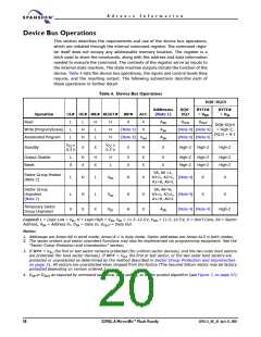
Word/Byte Configuration
The BYTE# pin controls whether the device data I/O pins operate in the byte or
word configuration. If the BYTE# pin is set at logic 1, the device is in word con-
figuration, DQ0–DQ15 are active and controlled by CE# and OE#.
If the BYTE# pin is set at logic 0, the device is in byte configuration, and only
data I/O pins DQ0–DQ7 are active and controlled by CE# and OE#. The data I/
O pins DQ8–DQ14 are tri-stated, and the DQ15 pin is used as an input for the
LSB (A-1) address function.
Requirements for Reading Array Data
To read array data from the outputs, the system must drive the CE# and OE#
pins to V . CE# is the power control and selects the device. OE# is the output
IL
control and gates array data to the output pins. WE# should remain at V
.
IH
The internal state machine is set for reading array data upon device power-up,
or after a hardware reset. This ensures that no spurious alteration of the mem-
ory content occurs during the power transition. No command is necessary in this
mode to obtain array data. Standard microprocessor read cycles that assert valid
addresses on the device address inputs produce valid data on the device data
outputs. The device remains enabled for read access until the command register
contents are altered.
See Reading Array Data on page 43 for more information. Refer to the AC Read-
Only Operations table for timing specifications and the timing diagram. Refer to
the DC Characteristics table for the active current specification on reading array
data.
Page Mode Read
The device is capable of fast page mode read and is compatible with the page
mode Mask ROM read operation. This mode provides faster read access speed
for random locations within a page. The page size of the device is 4 words/8
bytes. The appropriate page is selected by the higher address bits A(max)–A2.
Address bits A1–A0 in word mode (A1–A-1 in byte mode) determine the specific
word within a page. This is an asynchronous operation; the microprocessor sup-
plies the specific word location.
The random or initial page access is equal to t
or t
and subsequent page
CE
ACC
read accesses (as long as the locations specified by the microprocessor falls
within that page) is equivalent to t . When CE# is deasserted and reasserted
PACC
for a subsequent access, the access time is t
or t . Fast page mode accesses
CE
ACC
are obtained by keeping the read-page addresses constant and changing the
intra-read page addresses.
Writing Commands/Command Sequences
To write a command or command sequence (which includes programming data
to the device and erasing sectors of memory), the system must drive WE# and
CE# to V , and OE# to V
.
IH
IL
The device features an Unlock Bypass mode to facilitate faster programming.
Once the device enters the Unlock Bypass mode, only two write cycles are re-
quired to program a word, instead of four. The Word Program Command
Sequence on page 44 contains details on programming data to the device using
both standard and Unlock Bypass command sequences.
April 22, 2005 S29GL-A_00_A3
S29GL-A MirrorBit™ Flash Family
19

 SPANSION [ SPANSION ]