A d v a n c e I n f o r m a t i o n
An erase operation can erase one sector, multiple sectors, or the entire device.
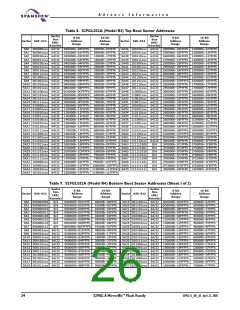
Tables 7 – 25 indicate the address space that each sector occupies.
Refer to the DC Characteristics table for the active current specification for the
write mode. The AC Characteristics section contains timing specification tables
and timing diagrams for write operations.
Write Buffer
Write Buffer Programming allows the system write to a maximum of 16 words/
32 bytes in one programming operation. This results in faster effective program-
ming time than the standard programming algorithms. See Write Buffer on
page 20 for more information.
Accelerated Program Operation
The device offers accelerated program operations through the ACC function. This
is one of two functions provided by the WP#/ACC or ACC pin, depending on
model number. This function is primarily intended to allow faster manufacturing
throughput at the factory.
If the system asserts V
on this pin, the device automatically enters the afore-
HH
mentioned Unlock Bypass mode, temporarily unprotects any protected sector
groups, and uses the higher voltage on the pin to reduce the time required for
program operations. The system would use a two-cycle program command se-
quence as required by the Unlock Bypass mode. Removing V
from the WP#/
HH
ACC or ACC pin, depending on model number, returns the device to normal op-
eration. Note that the WP#/ACC or ACC pin must not be at V for operations
HH
other than accelerated programming, or device damage may result. WP# con-
tains an internal pullup; when unconnected, WP# is at V
.
IH
Autoselect Functions
If the system writes the autoselect command sequence, the device enters the
autoselect mode. The system can then read autoselect codes from the internal
register (which is separate from the memory array) on DQ7–DQ0. Standard read
cycle timings apply in this mode. Refer to Autoselect Mode on page 30 and Au-
toselect Command Sequence on page 44 for more information.
Standby Mode
When the system is not reading or writing to the device, it can place the device
in the standby mode. In this mode, current consumption is greatly reduced, and
the outputs are placed in the high impedance state, independent of the OE#
input.
The device enters the CMOS standby mode when the CE# and RESET# pins are
both held at V ± 0.3 V. (Note that this is a more restricted voltage range than
IO
V
.) If CE# and RESET# are held at V , but not within V ± 0.3 V, the device
IH IO
IH
is in the standby mode, but the standby current is greater. The device requires
standard access time (t ) for read access when the device is in either of these
CE
standby modes, before it is ready to read data.
If the device is deselected during erasure or programming, the device draws ac-
tive current until the operation is completed.
Refer to the DC Characteristics on page 64 for the standby current specification.
20
S29GL-A MirrorBit™ Flash Family
S29GL-A_00_A3 April 22, 2005

 SPANSION [ SPANSION ]